Theory
Like the Half Adder, a Full Adder counts it’s inputs. The full Adder counts three of them though. This to account for the carry in of the previous bit.
Truth Table
| iA | iB | iC | oS | oC |
|---|---|---|---|---|
| 0 | 0 | 0 | 0 | 0 |
| 0 | 0 | 1 | 1 | 0 |
| 0 | 1 | 0 | 1 | 0 |
| 0 | 1 | 1 | 0 | 1 |
| 1 | 0 | 0 | 1 | 0 |
| 1 | 0 | 1 | 0 | 1 |
| 1 | 1 | 0 | 0 | 1 |
| 1 | 1 | 1 | 1 | 1 |
Design
Once more, we’ll start with the truth table, derive sum-of-product equations, and circuit-ize.
oS = (iA'*iB'*iC) + (iA'*iB*iC') + (iA*iB'*iC') + (iA*iB*iC)
oC = (iA'*iB*iC) + (iA*iB'*iC) + (iA*iB*iC') + (iA*iB*iC)
Again, we need to convert these into NCL logic (DATA0 and DATA1).
oS.0 = (iA.0*iB.0*iC.0)+(iA.0*iB.1*iC.1)+(iA.1*iB.0*iC.1)+(iA.1*iB.1*iC.0)
oS.1 = (iA.0*iB.0*iC.1)+(iA.0*iB.1*iC.0)+(iA.1*iB.0*iC.0)+(iA.1*iB.1*iC.1)
oC.0 = (iA.0*iB.0*iC.0)+(iA.0*iB.0*iC.1)+(iA.0*iB.1*iC.0)+(iA.1*iB.0*iC.0)
oC.1 = (iA.0*iB.1*iC.1)+(iA.1*iB.0*iC.1)+(iA.1*iB.1*iC.0)+(iA.1*iB.1*iC.1)
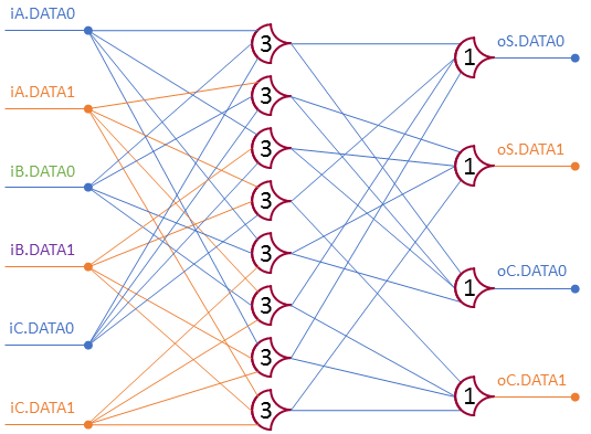
Note that each row of the truth table is used exactly twice, once for each variable. Since 0’s and 1’s are both represented by a high signal, each output variable {oS, oC} has an assignment for each case. Build the AND-Plane with TH33 gates, and the OR-Plane with TH13 gates:

This design takes up 168 transistors in total. Lets see if we can make it with fewer.
Optimization
This time, instead of SOP form, I’m going to look at it more intuitively. Since the bits are symmetric (the values of iA can be swapped with iB without any change in the expected output) let’s look at counting them with threshold gates instead of checking individual cases. To check a ‘less than’ relation ship for number of inputs set, just count the number of 0’s.
oS.1: (1 <= NumBits < 2) + (3 <= NumBits) --5 gates
oS.0: (NumBits < 1) + (2 <= NumBits < 3)  --5 gates

oC.1: (2 <= NumBits)                      -- 1 gate (shared)
oC.0: (NumBits < 2)                       -- 1 gate (shared)
Gate version:
oS.1:
TH12(
     TH22(
          TH13(iA.1, iB.1, iC.1),  -- 1 <= NumBits
          TH23(iA.0, iB.0, iC.0)), -- NumBits < 2
     TH33(iA.1, iB.1, iC.1))); -- 3 <= NumBits

oS.0:
TH12(
     TH33(iA.0, iB.0, iC.0), -- NumBits < 1
     TH22(
          TH23(iA.1, iB.1, iC.1),  -- 2 <= NumBits
          TH13(iA.0, iA.0, iA.0)); -- NumBits < 3

oC.1: TH23(iA.1, iB.1, iC.1) -- 2 <= NumBits
oC.0: TH23(iA.0, iB.0, iC.0) -- NumBits < 2
I’m going to call this ‘functional notation’. It treats each gate as a function with other gates as inputs; common expressions are evaluated only once (duplicate gates are only built once, then shared). This uses the following gates (with their transistor counts):
3 TH12 = 3*6 = 18 transistors1 TH22 = 1*12 = 12 transistors2 TH13 = 2*8 = 16 transistors2 TH23 = 2*18 = 36 transistors2 TH33 = 2*16 = 32 transistors
Total: 114 transistors (-32% from SOP). The downside is that this is three-layer logic, which generally has a little higher delay for that third layer. On the upside, most of the gates have fewer inputs (2 and 3 inputs instead of 3 and 4 inputs). This reduces the complexity of each gate and may actually reduce the critical path. I won’t do that analysis here.
You might be tempted to obtain the *.0 or *.1 signal by inverting the other. You cannot do this in NCL. You must be able to pass on NULL wavefronts which require both to be 0. This is a downside of NCL, all groups require two (or more) complimentary circuits to obtain. This limitation results in increased die area.
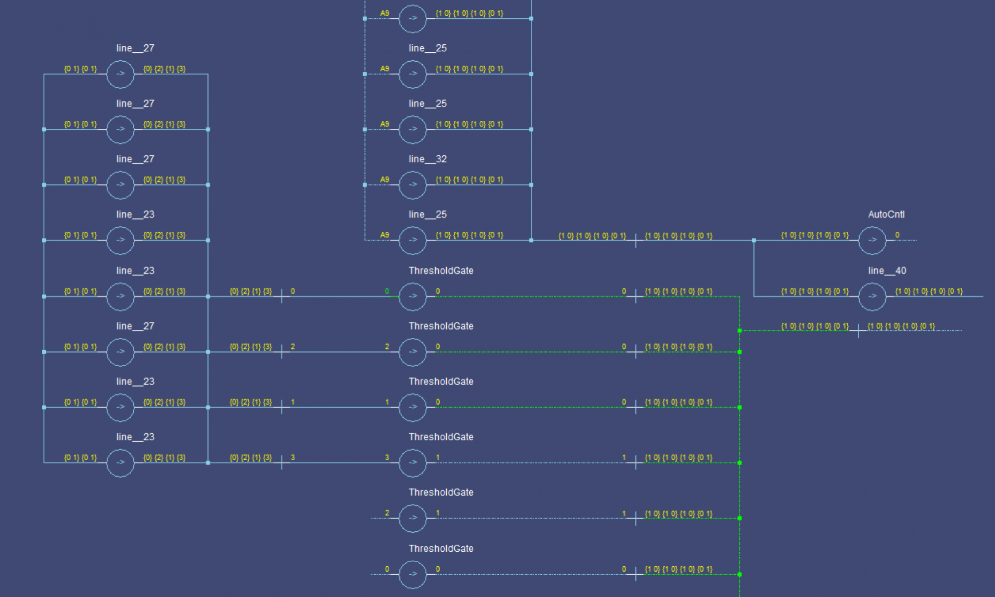
See my next post for the implementation.


One Reply to “NCL Full Adder Design”