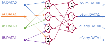
Design Recap
The circuit from my last post:
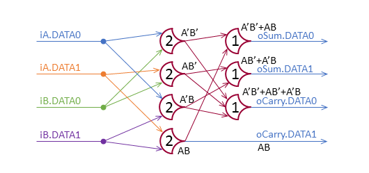
oS.1:
TH12(
  TH22(
    TH13(iA.1, iB.1, iC.1), -- 1 <= NumBits
    TH23(iA.0, iB.0, iC.0)), -- NumBits < 2
  TH33(iA.1, iB.1, iC.1))); -- 3 <= NumBits

oS.0:
TH12(
  TH33(iA.0, iB.0, iC.0), -- NumBits < 1
  TH22(
    TH23(iA.1, iB.1, iC.1), -- 2 <= NumBits
    TH13(iA.0, iA.0, iA.0)); -- NumBits < 3

oC.1: TH23(iA.1, iB.1, iC.1) -- 2 <= NumBits

oC.0: TH23(iA.0, iB.0, iC.0) -- NumBits < 2
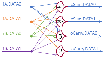
Optimized
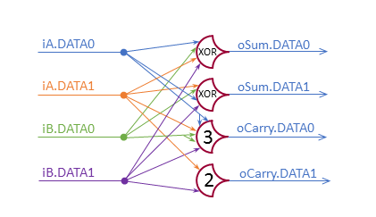
The structural VHDL implementation:
library ieee;
use ieee.std_logic_1164.all;
use ieee.numeric_std.all;
use work.ncl.all;

entity FullAdder is
  port(iC : in ncl_pair;
       a : in ncl_pair;
       b : in ncl_pair;
       oS : out ncl_pair;
       oC : out ncl_pair);
end FullAdder;

architecture structural of FullAdder is
  type first_layer is array (integer range <>) of std_logic_vector(0 to 2);
  signal first_layer_inputs : first_layer(0 to 7);
  signal intermediate : std_logic_vector(0 to 7);
  signal inputs : ncl_pair_vector(0 to 2);

begin
  inputs(2) <= a;
  inputs(1) <= b;
  inputs(0) <= iC;
  input_layer: for i in 0 to 7 generate
    bits: for ibit in 0 to 2 generate
      Input0Selection: if (to_unsigned(2**iBit, 3) and to_unsigned(i, 3)) = 0 generate
        first_layer_inputs(i)(iBit) <= inputs(iBit).Data0;
      end generate;
      Input1Selection: if (to_unsigned(2**iBit, 3) and to_unsigned(i, 3)) > 0 generate
        first_layer_inputs(i)(iBit) <= inputs(iBit).Data1;
      end generate;
    end generate;
    gate: THmn
            generic map(M => 3, N => 3)
            port map(inputs => first_layer_inputs(i),
                     output => intermediate(i));
  end generate;

  oS0: THmn
         generic map(M => 1, N => 4)
         port map(inputs(0) => intermediate(0),
                  inputs(1) => intermediate(3),
                  inputs(2) => intermediate(5),
                  inputs(3) => intermediate(6),
                  output => oS.DATA0);

  oS1: THmn
         generic map(M => 1, N => 4)
         port map(inputs(0) => intermediate(1),
                  inputs(1) => intermediate(2),
                  inputs(2) => intermediate(4),
                  inputs(3) => intermediate(7),
                  output => oS.DATA1);

  oC0: THmn
         generic map(M => 1, N => 4)
         port map(inputs(0) => intermediate(0),
                  inputs(1) => intermediate(1),
                  inputs(2) => intermediate(2),
                  inputs(3) => intermediate(4),
                  output => oC.DATA0);

  oC1: THmn
         generic map(M => 1, N => 4)
         port map(inputs(0) => intermediate(3),
                  inputs(1) => intermediate(5),
                  inputs(2) => intermediate(6),
                  inputs(3) => intermediate(7),
                  output => oC.DATA1);
end structural;

architecture optimized of FullAdder is
  signal sLT2 : std_logic;
  signal sLT3 : std_logic;
  signal sGE2 : std_logic;
  signal sGE1 : std_logic;
  signal sEQ3 : std_logic;
  signal sEQ2 : std_logic;
  signal sEQ1 : std_logic;
  signal sEQ0 : std_logic;
begin
  LT2: THmn
         generic map(M => 2, N => 3)
         port map(inputs(0) => a.DATA0,
                  inputs(1) => b.DATA0,
                  inputs(2) => iC.DATA0,
                  output => sLT2);

  GE2: THmn
         generic map(M => 2, N => 3)
         port map(inputs(0) => a.DATA1,
                  inputs(1) => b.DATA1,
                  inputs(2) => iC.DATA1,
                  output => sGE2);

  GE1: THmn
         generic map(M => 1, N => 3)
         port map(inputs(0) => a.DATA1,
                  inputs(1) => b.DATA1,
                  inputs(2) => iC.DATA1,
                  output => sGE1);

  EQ1: THmn
         generic map(M => 2, N => 2)
         port map(inputs(0) => sGE1,
                  inputs(1) => sLT2,
                  output => sEQ1);

  EQ3: THmn
         generic map(M => 3, N => 3)
         port map(inputs(0) => a.DATA1,
                  inputs(1) => b.DATA1,
                  inputs(2) => iC.DATA1,
                  output => sEQ3);

  S1: THmn
        generic map(M => 1, N => 2)
        port map(inputs(0) => sEQ1,
                 inputs(1) => sEQ3,
                 output => oS.DATA1);

  EQ0: THmn
         generic map(M => 3, N => 3)
         port map(inputs(0) => a.DATA0,
                  inputs(1) => b.DATA0,
                  inputs(2) => iC.DATA0,
                  output => sEQ0);

  LT3: THmn
         generic map(M => 1, N => 3)
         port map(inputs(0) => a.DATA0,
                  inputs(1) => b.DATA0,
                  inputs(2) => iC.DATA0,
                  output => sLT3);

  EQ2: THmn
         generic map(M => 2, N => 2)
         port map(inputs(0) => sGE2,
                  inputs(1) => sLT3,
                  output => sEQ2);

  S0: THmn
        generic map(M => 1, N => 2)
        port map(inputs(0) => sEQ2,
                 inputs(1) => sEQ0,
                 output => oS.DATA0);

  oC.DATA0 <= sLT2;
  oC.DATA1 <= sGE2;

end optimized;
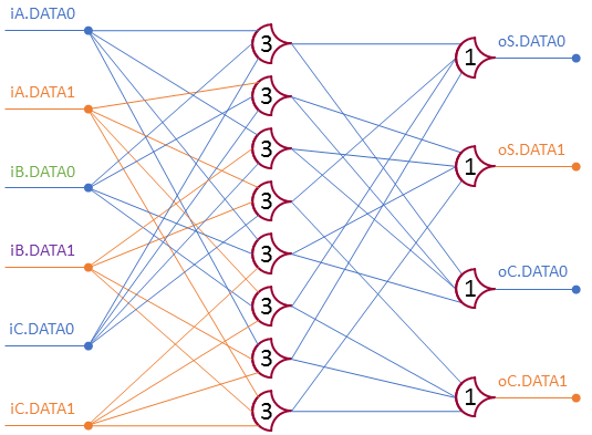
This VHDL implementation of the the un-optimized design uses generic loops to setup the first layer (the first layer uses all combinations of group values). The second layer is set up manually.
The optimized design’s signals are named in terms of relations Greater or Equal to #, Less Than #, and EQual to #. So sEQ1 is asserted when 1 input group is set to 1, and sGE2 is asserted when at least 2 input groups are set to 1.
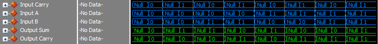
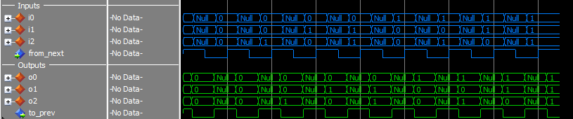
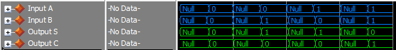
Testing
The test script runs through all combinations of inputs. I ran the tests with both versions. Here’s the result, no surprises really.