I am transitioning back into school, and might not post for a bit.
Sorry.
An assortment of technical content
I am transitioning back into school, and might not post for a bit.
Sorry.
A Shifter takes an array of bits, and shifts them right of left. Numerically, this is like multiplying or dividing by 2 (in the case of binary numbers). Some examples:
| Direction | Input | Shift Amount | Output |
|---|---|---|---|
| Right | 001001 |
1 | 000100 |
| Left | 001001 |
1 | 010010 |
| Right | 001001 |
2 | 000010 |
| Left | 001001 |
3 | 001000 |
This could be applied to non-binary variables as well (like 3-rail signals) but the exact meaning will be different. There are a few ‘extensions’ to this behavior I’d like to add:
Rotation allows the bits shifted out one end to be shifted back in the other:
| Direction | Input | Output |
|---|---|---|
| Right | 1001 |
1100 |
| Left | 1001 |
0011 |
Arithmetic shifting treats the shift as a mathematical operation and preserves the sign of the number. It is only valid for right shifts.
| Direction | Input | Output |
|---|---|---|
| Right | 100(-4) |
110(-2) |
| Right | 110(-2) |
111(-1) |
The sign of a number is represented by leading 1’s in the MSB, so an arithmetic right shift adds 1’s into the leftmost bits, if the number was negative. This is accomplished by shifting in the MSB.
Each shift_amount bit corresponds to a shift of 2^n, where n is the index of the bit. Each constant-size shift can be accomplished with only wiring. As my CprE 381 professor always said, if you have two possible values, the easiest way to pick one is a MUX. So, each shift_amount bit will choose between an unshifted, or 2^n shifted value. By connecting these in layers, we get a shift of any size.
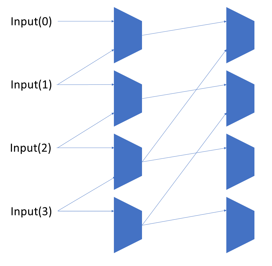
The un-supplied inputs are 0’s. The first column is controlled by shift_amount(0), the second column is controlled by shift_amount(1).
To change the direction, we add a mux at the beginning that selects a reversed version of the input, let the shifter shift that, then un-reverse it at the end.
To add rotations, we add another input to the MUX’s at the bottom that feeds back from the top, so that the ‘lost’ bits are shifted back in.
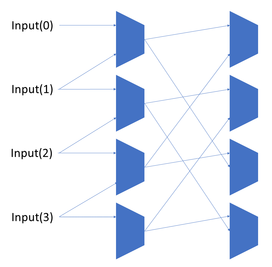
To add arithmetic operations, the unassigned inputs in the lower MUX’s are changed from 0 to the MSB of the input. This signal is constant across all the MUX’s it is applied to, so it is generated with a single MUX. On a left shift, the shifted-in value must be 0, so the MUX can only output the MSB when a right arithmetic shift is selected.
the VHDL source, using generics to make it work for any number of inputs (even non-powers of 2, btw):
library ieee;
use work.ncl.all;
use ieee.std_logic_1164.all;

entity Shifter is
  generic(NumInputs : integer := 2);
  port(inputs       : in ncl_pair_vector(0 to NumInputs - 1);
       shift_amount : in ncl_pair_vector(0 to clog2(NumInputs) - 1);
       direction    : in ncl_pair;
       rotate       : in ncl_pair;
       logical      : in ncl_pair;
       output       : out ncl_pair_vector(0 to NumInputs - 1));
end Shifter;

architecture structural of Shifter is
  constant NumShiftAmountBits : integer := clog2(NumInputs);
  constant NumRows : integer := clog2(NumInputs);

  type RowSignals is array (integer range <>) of ncl_pair_vector(0 to NumInputs - 1);

  -- The shifted array at each stage of the shifter.
  signal rows : RowSignals(0 to NumRows);

  -- A generated value that is always DATA0 or NULL as appropriate
  signal zero_in : ncl_pair;

  -- The third input that is used for either logical or arithmetic operations.
  signal non_rotate_in : ncl_pair;

  signal input_reversed : ncl_pair_vector(0 to NumInputs - 1);
  signal output_reversed : ncl_pair_vector(0 to NumInputs - 1);

begin

  produceDATA0: THmn
    generic map(M => 1, N => 2)
    port map(inputs(0) => inputs(0).DATA0,
             inputs(1) => inputs(0).DATA1,
             output => zero_in.DATA0);

  zero_in.DATA1 <= '0';   msb_in_mux: MUX     generic map(NumInputs => 4)
    port map(iOptions(0) => inputs(NumInputs-1),
             iOptions(1) => zero_in,
             iOptions(2) => zero_in,
             iOptions(3) => zero_in,
             iSel(0) => logical,
             iSel(1) => direction,
             output => non_rotate_in);

  in_bit_flipper: for i in 0 to NumInputs-1 generate
    input_reversed(i) <= inputs(NumInputs-1-i);     directionMux: MUX       generic map(NumInputs => 2)
      port map(iOptions(0) => inputs(i),
               iOptions(1) => input_reversed(i),
               iSel(0) => direction,
               output => rows(0)(i));
  end generate;

--  rows(0) <= inputs;

  rowsloop: for r in 0 to NumRows-1 generate
    columns: for c in 0 to NumInputs-1 generate
      ifstd: if (c + (2**r)) < NumInputs generate         multiplexer: MUX           generic map(NumInputs => 2)
          port map(iOptions(0) => rows(r)(c),
                   iOptions(1) => rows(r)(c + (2**r)),
                   iSel(0) => shift_amount(r),
                   output => rows(r+1)(c));

      end generate;

      ifwrp: if (c + (2**r)) >= NumInputs generate
        multiplexer: MUX
          generic map(NumInputs => 4)
          port map(iOptions(0) => rows(r)(c),
                   iOptions(1) => non_rotate_in,
                   iOptions(2) => rows(r)(c),
                   iOptions(3) => rows(r)((c+(2**r)) mod NumInputs),
                   iSel(0) => shift_amount(r),
                   iSel(1) => rotate,
                   output => rows(r+1)(c));

      end generate;
    end generate;
  end generate;

  out_bit_flipper: for i in 0 to NumInputs-1 generate
    output_reversed(i) <= rows(NumRows)(NumInputs - 1 - i);     outMux: MUX       generic map(NumInputs => 2)
      port map(iOptions(0) => rows(NumRows)(i),
               iOptions(1) => output_reversed(i),
               iSel(0) => direction,
               output => output(i));
  end generate;

end structural;
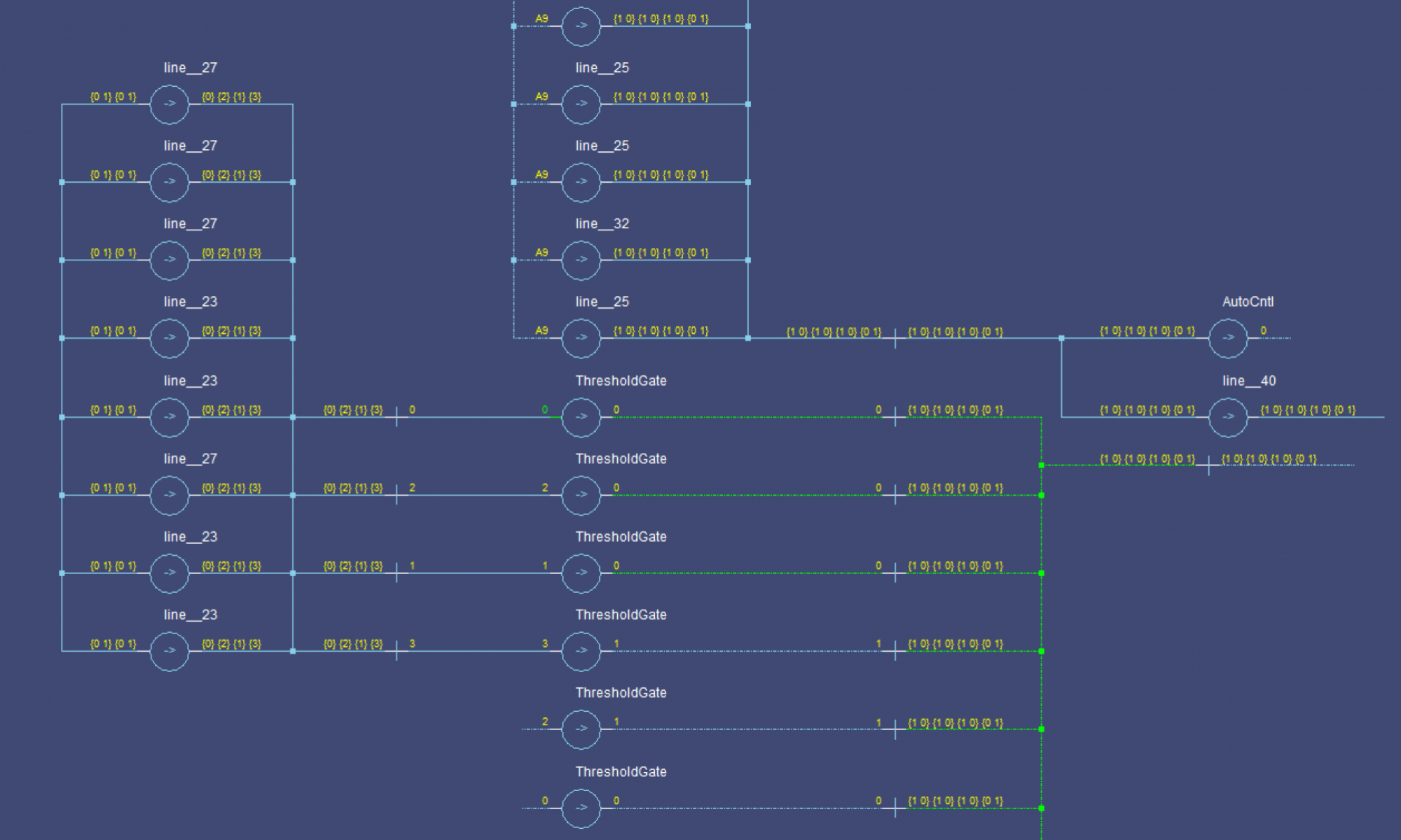
This code generates the necessary multiplexers for shifting the signal, flipping it at the input and output, and selecting how to handle the bits that can’t be shifted normally (because the source is out of range).
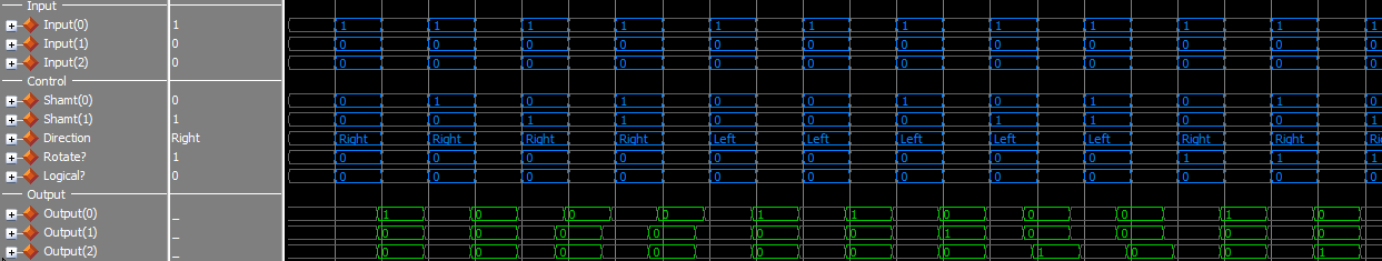
I made a simple test script to run through some cases. Everything seems to check out, here’s a sample:
My naming conventions have probably been misleading. I have mostly treated NCL bits as three-state logic (NULL, DATA0, and DATA1) this is a valid way to work with the data, but it is limiting. The better way to think of it is as individual 2-state logic lines (NULL and DATA).
Internally to a component, using single-rail signals is very helpful. Not only are single-rail signals the inputs to all NCL gates, but they can be used as links between components as well. Single-rail signals cannot really be passed through registers because they have to be asserted for the DATA wave to read as complete. This would prevent the signal from conveying meaning, as it would always have the same value during computations.
This section is unverified theory. Please share your thoughts below.
I will b using _ to refer to a non-asserted rail (null) and ^ to refer to an asserted rail (data).
Another benefit of this view is that you get more flexibility in state encodings. Standard encodings (that I’ve come across) use mutually exclusive data lines. So a 3-rail signal would have 3 possible states and a 4-rail signal would have 4 states. By thinking of the data more in terms of DATA and NULL, you get to design your own state encodings. For example, with a 4-rail encoding, you could use the following 6 states: {__^^, _^_^, _^^_, ^__^, ^_^_, ^^__}.
A state space is the set of valid states. We will use it here a little more specifically to refer to the valid DATA states. Not all state spaces will actually work for NCL, The completion logic has to be able to correctly identify completed states. For example, if we try to use the following for a 3-rail signal, we have a problem: {__^, _^^, ^^^}. If the result is the last state (^^^) and the data on line 0 arrives first, the completion logic will see it as a complete __^ and pass on the wrong result.
For any state, it has to be able to partially arrive, without looking like another state. This is required for delay insensitivity. A simple way to make this happen is to use M-hot states. By that I mean that each state will have the same number of rails asserted as data (^), and all such states can be used. The number of states in such an assignment for a N-rail signal is M Choose N or C(M, N). This has its maximum value when M=N/2. It also has the benefit that any incomplete state has at most M-1 rails set, which will never match another state.
The logic proof-y version: ∀x,y∈S:(x&y!=x) and (x&y!=y) must hold (& is the bitwise AND operator) where S is the state space.
Using this N/2-hot encoding, the states/rail is
| Rails | States | State Increase Factor |
|---|---|---|
| 1 | 1 | |
| 2 | 2 | 2 |
| 3 | 3 | 1.5 |
| 4 | 6 | 2 |
| 5 | 10 | 1.6667 |
| 6 | 20 | 2 |
Using this encoding, you get nearly twice as many states for each rail you add. Using mutually-exclusive rails (1-hot) you get 1 extra state per rail. Even if you break it up into 2-rail pairs and use combinations of those values, you only double your state space for every 2 rails you add. In the table above, s you increase the number of rails, the factor approaches 2 for the odd numbers of rails as well.
In special cases, you might want a more complex encoding, some examples of valid state spaces:
{___^, ^_^_, _^__}{__^^, ^___, _^__}{^^^_, ^^_^, ^_^^, _^^^}{^^^_, ___^}{__^^, _^_^, _^^_, ^__^, ^_^_, ^^__}While you can increase the compatibility of your modules by using a standard state space, sometimes you can reduce the number of rails by using more dense encodings. Additionally, signals that exist only between registers (are not passed on) can actually be 1-rail signals, which is something I have a hard time remembering when integrating components. These 1-rail signals can act as enable signals: They can be used to prevent data from propagating, or to allow it to propagate (remember steering).
In Null Convention Logic, all computation is done with oscillating DATA/NULL cycles. The NULL cycles clear the whole circuit, the DATA cycles perform the computation. This requires 2 transition sets per computation (Previous DATA => NULL => Next DATA). Sometimes the DATA output from a component will not be used (think the unselected inputs of a MUX).
When using steering, the DATA wavefront is only passed to the necessary components. In the case of a MUX, the outputs of these components are then combined as needed with TH1n gates:
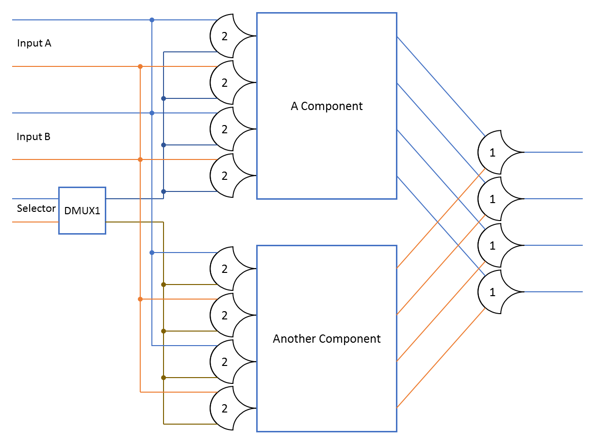
The TH22 gates in this example do not allow the DATA wavefront to apss into the components unless they are selected by the DMUX1. During any particular DATA wavefront, only one of these components will be active at a time; the other component will remain NULL. This saves transitions, and thus power. This method also works if only some, or no inputs are shared.
The DMUX1 component is a decoder, that only outputs the DATA1 lines. Technically, I think it matches the NCL network criteria, if you consider the outputs to be single rail outputs, which have only one DATA value. The DMUX1 is used to enable only the selected component.
We will use steering when our ALU has more than just the Adder with glue logic. At some point we’ll have a multiplier, and a shifter, only one of these will operate at a time.
For more on steering, see Karl Fant’s site. His blog posts have lots of good theory too.
An arithmetic logic unit (ALU) is a component that performs operations on (usually) two or more sets of inputs, and outputs results. The operation performed is designated by an Operation signal.
Our ALU will start simple, and we’ll add more operations over time. First, let’s build an add/sub unit. I already have an adder, which can be used to subtract by swapping some signals: In single-rail (standard) logic, to subtract instead of add, the second input to the adder is inverted and the carry bit is set – in NCL, we invert the input by swapping DATA0 and DATA1.
The swapper operates as the following equations
output.0 = input.0*swap.0 + input.1*swap.1
output.1 = input.1*swap.0 + input.0*swap.1
These can be implemented with THxor0 gates:
output.0 = THxor0(input.0, swap.0, input.1, swap.1)
output.1 = THxor0(input.1, swap.0, input.0, swap.1)
Our add/sub module will have these on every bit on input to the adder, with iC having the swap signal fed directly into it. Swap will be exposed in the component’s port as the add/subtract selector:
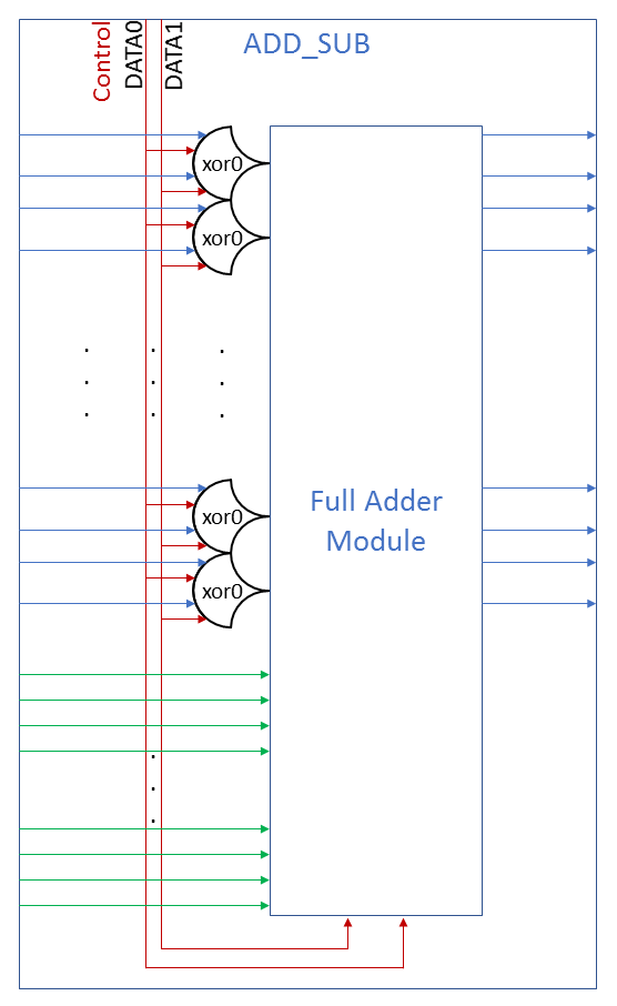
Green is iA, blue is iB, and red is iC on the Adder. If Control is asserted (DATA1) iB will be inverted and the carry in will be asserted as well, resulting in subtraction.
This module actually fulfills the interface of an ALU by itself, it has data inputs, and a opcode. When we add more operations, we’ll wrap it all up in a ALU block and add a MUX.
To implement this in VHDL, we need 1 Adder module and 2*N THxor0 gates:
use ieee.std_logic_1164.all;
use ieee.numeric_std.all;
use work.ncl.all;

entity AddSub is
  generic(NumBits : integer := 4);
  port(iA        : in ncl_pair_vector(0 to NumBits-1);
       iB        : in ncl_pair_vector(0 to NumBits-1);
       Operation : in ncl_pair;

       oS       : out ncl_pair_vector(0 to NumBits-1);
       oC       : out ncl_pair);
end AddSub;

architecture structural of AddSub is

  -- iB into adder, potentially inverted from entity input
  signal adder_iB : ncl_pair_vector(0 to NumBits-1);

begin

  plainAdder: Adder
    generic map(NumAdderBits => NumBits)
    port map(iC => Operation,
             iA => iA,
             iB => adder_iB,
             oS => oS,
             oC => oC);

  bits: for iBit in 0 to NumBits-1 generate

    inverter0: THxor0 -- DATA0, Potentially inverted
      port map(A => iB(iBit).DATA0,
               B => Operation.DATA0,
               C => iB(iBit).DATA1,
               D => Operation.DATA1,
               output => adder_iB(iBit).DATA0);

    inverter1: THxor0 -- DATA1, Potentially inverted
      port map(A => iB(iBit).DATA0,
               B => Operation.DATA1,
               C => iB(iBit).DATA1,
               D => Operation.DATA0,
               output => adder_iB(iBit).DATA1);

  end generate;

end structural;
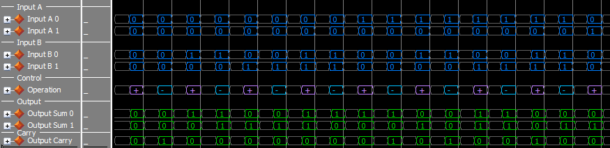
The 2-bit case above is a little small, but it runs quickly. I have tested the module up to 6 bits. To change the number of bits, change the number at the top of the test script. The first several cases (interpreted to decimal):
0+0=00-0=00+1=10-1=-10+2=20-2=-2This test script does check the sum output, but it does not verify the carry out.
Commit: 55d8c9f