See this post for the theory and design of the NCL Half Adder.
Design Recap
Here’s the circuit design:
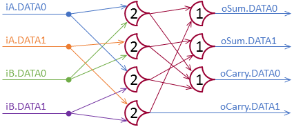
(simple version)
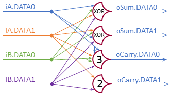
(optimized version)
The top two gates are THxor0 gates, the next is a TH34w22, and the last one is a TH22 gate. I will implement this structurally, a fairly straightforward process in this case.
Implementation
library ieee;
use ieee.std_logic_1164.all;
use work.ncl.all;

entity HalfAdder is
 port(a : in ncl_pair;
      b : in ncl_pair;
      s : out ncl_pair;
      c : out ncl_pair);
end HalfAdder;

architecture structural of HalfAdder is
  signal a0b0_ins : std_logic_vector(0 to 1);
  signal a0b0_out : std_logic;
  signal a0b1_ins : std_logic_vector(0 to 1);
  signal a0b1_out : std_logic;
  signal a1b0_ins : std_logic_vector(0 to 1);
  signal a1b0_out : std_logic;
  signal a1b1_ins : std_logic_vector(0 to 1);
  signal a1b1_out : std_logic;

signal s0_ins : std_logic_vector(0 to 1);
  signal s0_out : std_logic;
  signal s1_ins : std_logic_vector(0 to 1);
  signal s1_out : std_logic;

  signal c0_ins : std_logic_vector(0 to 2);
  signal c0_out : std_logic;
begin
  a0b0_ins(0) <= a.DATA0;
  a0b0_ins(1) <= b.DATA0;   T21_A0B0 : THmn
               generic map(N => 2, M => 2)
               port map(inputs => a0b0_ins,
                        output => a0b0_out);

  a0b1_ins(0) <= a.DATA0;
  a0b1_ins(1) <= b.DATA1;   T21_A0B1 : THmn
               generic map(N => 2, M => 2)
               port map(inputs => a0b1_ins,
                        output => a0b1_out);

  a1b0_ins(0) <= a.DATA1;
  a1b0_ins(1) <= b.DATA0;   T21_A1B0 : THmn
               generic map(N => 2, M => 2)
               port map(inputs => a1b0_ins,
                        output => a1b0_out);

  a1b1_ins(0) <=  a.DATA1;
  a1b1_ins(1) <= b.DATA1;   T21_A1B1 : THmn
               generic map(N => 2, M => 2)
               port map(inputs => a1b1_ins,
                        output => a1b1_out);

  s1_ins(0) <= a0b1_out;
  s1_ins(1) <= a1b0_out;   T21_S1: THmn
            generic map(N => 2, M => 1)
            port map(inputs => s1_ins,
                     output => s1_out);
  s.DATA1 <= s1_out;

  s0_ins(0) <= a0b0_out;
  s0_ins(1) <= a1b1_out;   T21_S0: THmn
            generic map(N => 2, M => 1)
            port map(inputs => s0_ins,
                     output => s0_out);
  s.DATA0 <= s0_out;
  c.DATA1 <= a1b1_out;

  c0_ins(0) <= a1b0_out;
  c0_ins(1) <= a0b1_out;
  c0_ins(2) <= a0b0_out;   T31_C0: THmn
            generic map(N => 3, M => 1)
            port map(inputs => c0_ins,
                     output => c0_out);
  c.DATA0 <= c0_out;
end structural;

architecture optimized of HalfAdder is
begin
  Sum0: THxor0
          port map(A => A.DATA0,
                   B => B.DATA0,
                   C => A.DATA1,
                   D => B.DATA1,
                   output => s.DATA0);

  Sum1: THxor0
          port map(A => A.DATA1,
                   B => B.DATA0,
                   C => A.DATA0,
                   D => B.DATA1,
                   output => s.DATA1);

  Carry0: THmn
            generic map(N => 6, M => 3)
            port map(inputs(0) => A.DATA0,
                     inputs(1) => A.DATA0,
                     inputs(2) => B.DATA0,
                     inputs(3) => B.DATA0,
                     inputs(4) => A.DATA1,
                     inputs(5) => B.DATA1,
                     output => c.DATA0);

  Carry1: THmn
            generic map(N => 2, M => 2)
            port map(inputs(0) => A.DATA1,
                     inputs(1) => B.DATA1,
                     output => c.DATA1);
end optimized;
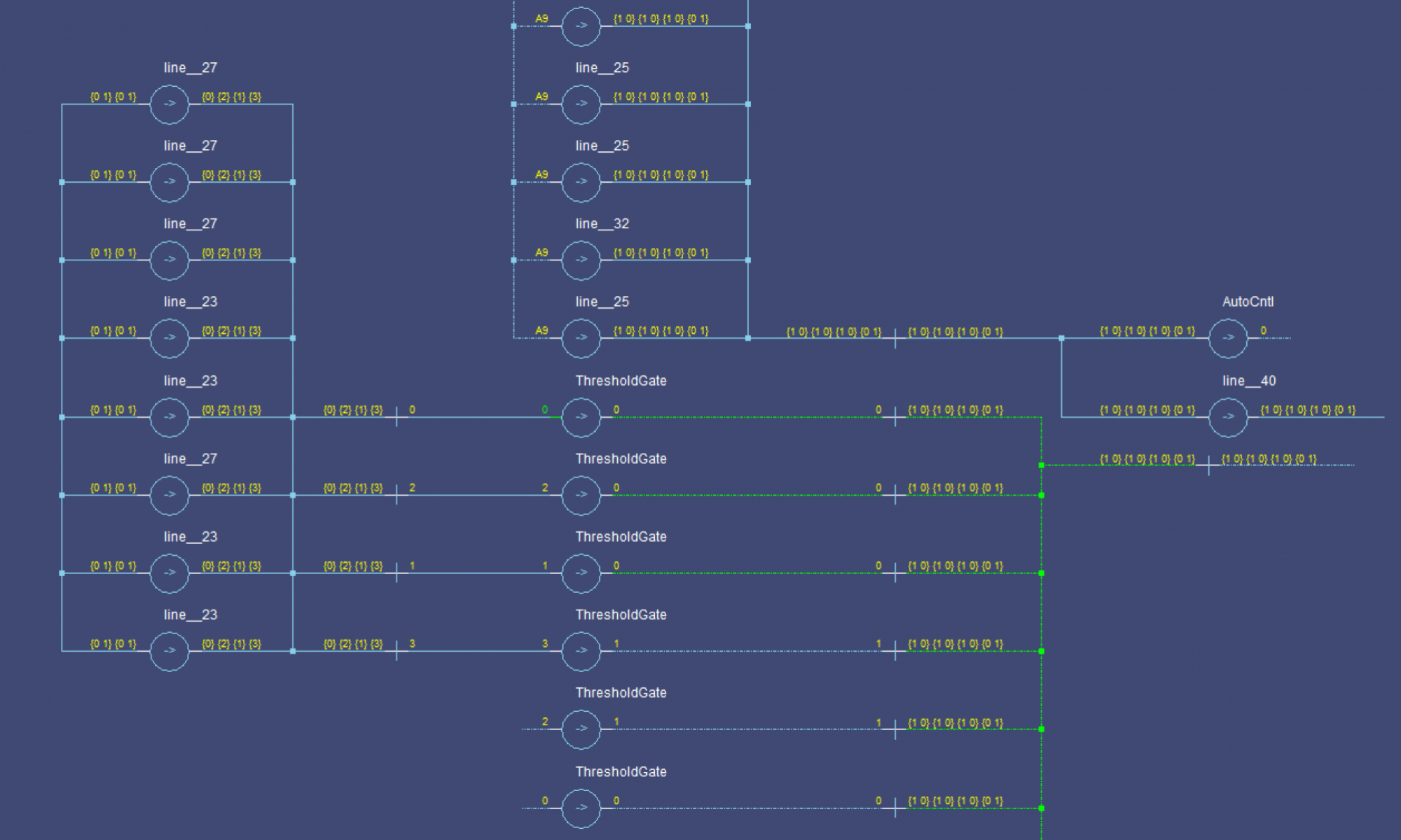
I have two implementations here. The basic version, and the optimized version. There’s not a lot to explain beyond VHDL syntax. The gates are built as in the diagram, though some orderings might have changed.
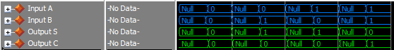
Testing
The test script runs through all input values, clearing to NULL in between. The test simulation run:
If you have any questions, leave a comment below.
Commit: a57125a
One Reply to “NCL Half Adder Implementation”