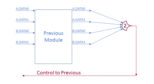
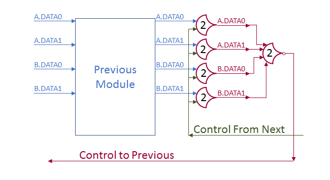
Design Recap
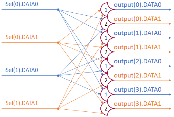
4-Option Example
for Case in 0 to N-1
[build CaseBits with DATA0's and DATA1's]
-- CaseBits is a concatenated signal from the iSelector input
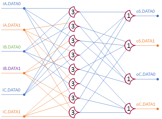
Selectors(Case) <= THNN(CaseBits)
GatedCase0 <= TH22(Selectors(Case), iOptions(Case).DATA0)
GatedCase1 <= TH22(Selectors(Case), iOptions(Case).DATA1)
next Case
output.DATA0 <= TH1N(Gated00, Gated10, Gated20, Gated30, ...)
output.DATA1 <= TH1N(Gated01, Gated11, Gated21, Gated31, ...)
Generic pseudo-VHDL
Implementation
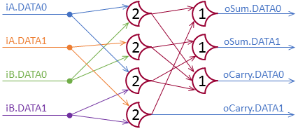
Remember the Full Adder‘s un-optimized version? If you look at the implementation, you’ll see a chunk of code at the top that generates one-hot encoding of all cases. We are going to use that for our internal Selectors signal:
cases: for case in 0 to NumOptions generate
  bits: for ibit in 0 to NumSelectors-1 generate

    Input0Selection: if (to_unsigned(2**iBit, 3) and to_unsigned(case, 3)) = 0 generate
      selectorInputs(case)(iBit) <= iOptions(case).DATA0;
    end generate;

    Input1Selection: if (to_unsigned(2**iBit, 3) and to_unsigned(case, 3)) > 0 generate
      selectorInputs(case)(iBit) <= iOptions(case).DATA1;
    end generate;
  end generate;

  CaseSelectorGate: THmn
    generic map(M => NumSelectors, N => NumSelectors)
    port map(inputs => selectorInputs(case),
             output => Selectors(case));

 end generate;
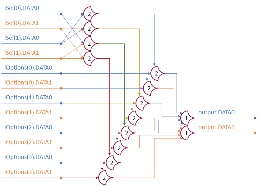
Next, we need to gate the two lines (DATA0 and DATA1) for each option, which will NULL them if they are not the selected signal:
cases: for case in 0 to NumOptions generate
  bits: for ibit in 0 to NumSelectors-1 generate

    Input0Selection: if (to_unsigned(2**iBit, 3) and to_unsigned(case, 3)) = 0 generate
      selectorInputs(case)(iBit) <= iOptions(case).DATA0;
    end generate;

    Input1Selection: if (to_unsigned(2**iBit, 3) and to_unsigned(case, 3)) > 0 generate
      selectorInputs(case)(iBit) <= iOptions(case).DATA1;
    end generate;
  end generate;

  CaseSelectorGate: THmn
    generic map(M => NumSelectors, N => NumSelectors)
    port map(inputs => selectorInputs(case),
             output => Selectors(case));

  Gated0: THmn
    generic map(M => 2, N => 2)
    port map(inputs(0) => Selectors(case),
             inputs(1) => iOptions(case).DATA0,
             output => GatedOptions0(case));

  Gated1: THmn
    generic map(M => 2, N => 2)
    port map(inputs(0) => Selectors(case),
             inputs(1) => iOptions(case).DATA1,
             output => GatedOptions1(case));

 end generate;
Finally, take all those gated options and or the signals together, so whichever one is selected will drive the line to a 1 if it is set:
cases: for case in 0 to NumOptions generate
  bits: for ibit in 0 to NumSelectors-1 generate

    Input0Selection: if (to_unsigned(2**iBit, 3) and to_unsigned(case, 3)) = 0 generate
      selectorInputs(case)(iBit) <= iOptions(case).DATA0;
    end generate;

    Input1Selection: if (to_unsigned(2**iBit, 3) and to_unsigned(case, 3)) > 0 generate
      selectorInputs(case)(iBit) <= iOptions(case).DATA1;
    end generate;
  end generate;

  CaseSelectorGate: THmn
    generic map(M => NumSelectors, N => NumSelectors)
    port map(inputs => selectorInputs(case),
             output => Selectors(case));

  Gated0: THmn
    generic map(M => 2, N => 2)
    port map(inputs(0) => Selectors(case),
             inputs(1) => iOptions(case).DATA0,
             output => GatedOptions0(case));

  Gated1: THmn
    generic map(M => 2, N => 2)
    port map(inputs(0) => Selectors(case),
             inputs(1) => iOptions(case).DATA1,
             output => GatedOptions1(case));

 end generate;

o0: THmn
  generic map(M => 1, N => NumOptions)
  port map(inputs(0) => GatedOptions0(case),
           output => output.DATA0);

o1: THmn
  generic map(M => 1, N => NumOptions)
  port map(inputs => GatedOptions1(case),
           output => output.DATA1);
That’s all the logic then, but we need to add the wrapping structures (entity declaration, architecture declaration, and internal signal declarations). This module will have one generic parameter (NumOptions), and a constant based on it (NumSelectors). The width of the iSelector input will be the log of the number of options:
entity MUX is
  generic(NumOptions : integer := 2);
  port (iSelector : in ncl_pair_vector(0 to clog2(NumOptions)-1);
        iOptions  : in ncl_pair_vector(0 to NumOptions1-);
        output   : out ncl_pair);
end MUX;

architecture structural of MUX is
  constant NumSelectors : integer := clog2(NumOptions);
  signal Selectors : std_logic_vector(0 to NumOptions-1);
  signal GatedOptions0 : std_logic_vector(0 to NumOptions-1);
  signal GatedOptions1 : std_logic_vector(0 to NumOptions-1);

  type SelectorData is array (integer range ) of std_logic_vector(0 to NumSelectors-1);
  signal selectorInputs : SelectorData(0 to NumOptions-1);
begin
  -- [This part is the same as before]

  cases: for case in 0 to NumOptions generate
    bits: for ibit in 0 to NumSelectors-1 generate

      Input0Selection: if (to_unsigned(2**iBit, 3) and to_unsigned(case, 3)) = 0 generate
        selectorInputs(case)(iBit) <= iOptions(case).DATA0;
      end generate;

      Input1Selection: if (to_unsigned(2**iBit, 3) and to_unsigned(case, 3)) > 0 generate
        selectorInputs(case)(iBit) <= iOptions(case).DATA1;
      end generate;

      CaseSelectorGate: THmn
        generic map(M => NumSelectors, N => NumSelectors)
        port map(inputs => selectorInputs(case),
                 output => Selectors(case));
    Gated0: THmn
      generic map(M => 2, N => 2)
      port map(inputs(0) => Selectors(case),
               inputs(1) => iOptions(case).DATA0,
               output => GatedOptions0(case));

    Gated1: THmn
      generic map(M => 2, N => 2)
      port map(inputs(0) => Selectors(case),
               inputs(1) => iOptions(case).DATA1,
               output => GatedOptions1(case));

    end generate;

  o0: THmn
    generic map(M => 1, N => NumOptions)
    port map(inputs(0) => GatedOptions0(case),
             output => output.DATA0);

  o1: THmn
    generic map(M => 1, N => NumOptions)
    port map(inputs => GatedOptions1(case),
             output => output.DATA1);

end structural;
Testing
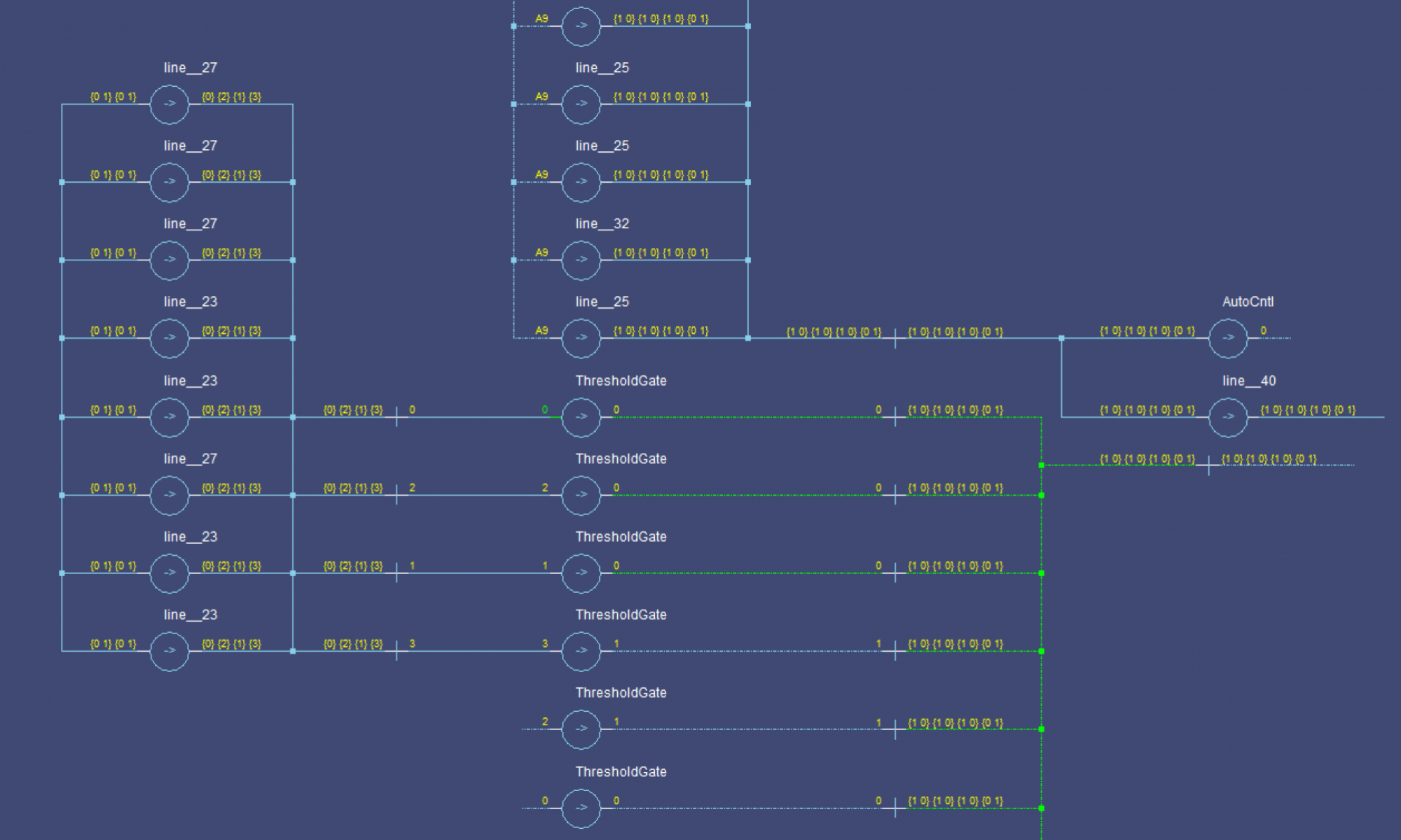
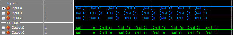
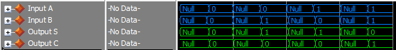
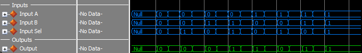
I am testing this module with 2 inputs for now; in theory it scales, but at some point I should add a 4-option test, and maybe a 5 to see how it does with non-power of 2 values. The test script goes through the inputs options and tests that they output correctly.
When I first ran this, I had an error where the outputs indexing was in the wrong order. I had the part of the code near the top messed up to use iSelectors(case).DATA0 instead of DATA1 and vice versa.
Commit: b35b729