NCL Full Adder Design

Theory

Like the Half Adder, a Full Adder counts it’s inputs. The full Adder counts three of them though. This to account for the carry in of the previous bit.

Truth Table

iA iB iC oS oC
0 0 0 0 0
0 0 1 1 0
0 1 0 1 0
0 1 1 0 1
1 0 0 1 0
1 0 1 0 1
1 1 0 0 1
1 1 1 1 1

Design

Once more, we’ll start with the truth table, derive sum-of-product equations, and circuit-ize.

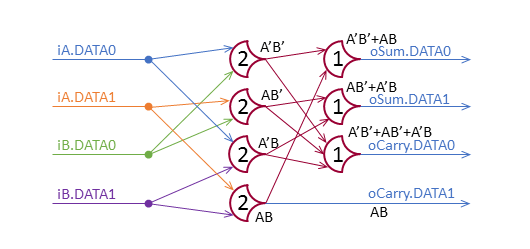
oS = (iA'*iB'*iC) + (iA'*iB*iC') + (iA*iB'*iC') + (iA*iB*iC)
oC = (iA'*iB*iC) + (iA*iB'*iC) + (iA*iB*iC') + (iA*iB*iC)

Again, we need to convert these into NCL logic (DATA0 and DATA1).

oS.0 = (iA.0*iB.0*iC.0)+(iA.0*iB.1*iC.1)+(iA.1*iB.0*iC.1)+(iA.1*iB.1*iC.0)
oS.1 = (iA.0*iB.0*iC.1)+(iA.0*iB.1*iC.0)+(iA.1*iB.0*iC.0)+(iA.1*iB.1*iC.1)
oC.0 = (iA.0*iB.0*iC.0)+(iA.0*iB.0*iC.1)+(iA.0*iB.1*iC.0)+(iA.1*iB.0*iC.0)
oC.1 = (iA.0*iB.1*iC.1)+(iA.1*iB.0*iC.1)+(iA.1*iB.1*iC.0)+(iA.1*iB.1*iC.1)

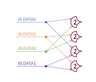
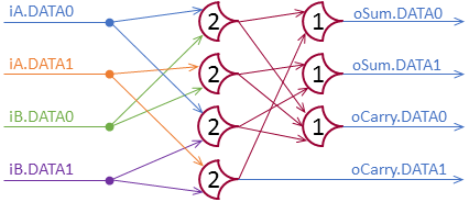
Note that each row of the truth table is used exactly twice, once for each variable. Since 0’s and 1’s are both represented by a high signal, each output variable {oS, oC} has an assignment for each case. Build the AND-Plane with TH33 gates, and the OR-Plane with TH13 gates:

FullAdder

This design takes up 168 transistors in total. Lets see if we can make it with fewer.

Optimization

This time, instead of SOP form, I’m going to look at it more intuitively. Since the bits are symmetric (the values of iA can be swapped with iB without any change in the  expected output) let’s look at counting them with threshold gates instead of checking individual cases. To check a ‘less than’ relation ship for number of inputs set, just count the number of 0’s.

oS.1: (1 <= NumBits < 2) + (3 <= NumBits) --5 gates
oS.0: (NumBits < 1) + (2 <= NumBits < 3)  --5 gates

oC.1: (2 <= NumBits)                      -- 1 gate (shared)
oC.0: (NumBits < 2)                       -- 1 gate (shared)

Gate version:

oS.1: 
TH12(
     TH22(
          TH13(iA.1, iB.1, iC.1),  -- 1 <= NumBits
          TH23(iA.0, iB.0, iC.0)), -- NumBits < 2
     TH33(iA.1, iB.1, iC.1))); -- 3 <= NumBits

oS.0:
TH12(
     TH33(iA.0, iB.0, iC.0), -- NumBits < 1
     TH22(
          TH23(iA.1, iB.1, iC.1),  -- 2 <= NumBits
          TH13(iA.0, iA.0, iA.0)); -- NumBits < 3

oC.1: TH23(iA.1, iB.1, iC.1) -- 2 <= NumBits
oC.0: TH23(iA.0, iB.0, iC.0) -- NumBits < 2

I’m going to call this ‘functional notation’. It treats each gate as a function with other gates as inputs; common expressions are evaluated only once (duplicate gates are only built once, then shared). This uses the following gates (with their transistor counts):

  • 3 TH12 = 3*6  = 18 transistors
  • 1 TH22 = 1*12 = 12 transistors
  • 2 TH13 = 2*8  = 16 transistors
  • 2 TH23 = 2*18 = 36 transistors
  • 2 TH33 = 2*16 = 32 transistors

Total: 114 transistors (-32% from SOP). The downside is that this is three-layer logic, which generally has a little higher delay for that third layer. On the upside, most of the gates have fewer inputs (2 and 3 inputs instead of 3 and 4 inputs). This reduces the complexity of each gate and may actually reduce the critical path. I won’t do that analysis here.

You might be tempted to obtain the *.0 or *.1 signal by inverting the other. You cannot do this in NCL. You must be able to pass on NULL wavefronts which require both to be 0. This is a downside of NCL, all groups require two (or more) complimentary circuits to obtain. This limitation results in increased die area.

See my next post for the implementation.

NCL Register Design

We’ve covered some basics on NCL (signals and gates), next I’m looking into registers and structuring a system with multiple components.

Theory

In synchronous logic, designers use flip-flops to store data, they store the current value on every clock edge, moving it to the next stage. In asynchronous logic, there is no clock edge, so saving data requires something else. NCL uses threshold gates as registers, which works because of their hysteresis property. The requirements for the register:

  • Hold on to the value for as long as the next module needs it
  • Send a reset (NULL) signal to the next module on all inputs when it needs it
  • Let the previous register know what it needs (DATA/NULL)

So, there’s handshaking going on here, each register tells the one before it what it needs, and tries to send the next one what it asks for.

Design

How do we send the request to the previous module then? Lets assume 1 control line, and see if we need something else later. Since we are representing NULL with 0, lets set a request for null to be 0, and a request for data to be 1. We want to receive data as soon as the module has reset to NULL, and we want NULL as soon as the module is outputting data on all groups. Here’s the initial design:

NCL Register

If both A and B have a line set (either 0 or 1) then the ‘watcher’ gate is set. The little circle on the tip is an inverter, it turns the 1 (indicating we have DATA) to a 0 (indicating we want NULL) and vice versa.

There is one more requirement: If the module after us is requesting DATA, we can’t store the NULL wavefront (which would overwrite the DATA values) and vice versa and so need to hold the previous module until we can. This means that the request has to be based on the register’s outputs, not its inputs.

Refresher: A group of NCL lines are the set of lines representing a single entity, only one can be active at a time, but it is allowable to have none active (NULL).

NCL Register

Here we have a gate saving each bit: If the control input is low, then the gates will reset when the previous module’s outputs clear (next module requesting null). If the control input is high, then the gates will save DATA inputs (next module requesting DATA).

When both groups (A and B) have data, the watcher sees 2 data lines, sets its output, which goes through the inverter and requests NULL (which won’t be saved until the next module requests NULL).

Eventually, the previous module NULLs out and waits for a DATA request. When the next module requests NULL, the register gates flip to NULLs and the watcher outputs a 0, which is inverted to a 1 (request for DATA). The NULL wavefront passes through the module to the next register.

This cycle continues.

Notes

Components can be directly linked without registers, but only one operation can occur between registers at a time. Adding the registers splits up the operation into smaller parts, which can occur in parallel (for different inputs). At the start, the first set of inputs is loaded, and when they move to the second stage, the first is NULLed, after that, the first stage receives the second set of inputs, while the first set is still running through the third stage. this continues, with all data wavefronts separated by NULL wavefronts.

NCL Half Adder Design

Definition

A Half Adder is a logic component that takes in two inputs, and outputs a binary (base 2) representation of how many are set (0, 1, or 2).

Like any good logic designer working on a small part, we’ll start by making a truth table:

iA iB oSum oCarry
0 0 0 0
0 1 1 0
1 0 1 0
1 1 0 1

Design

The first step of getting from truth table to gates is to generate Sum-of-Product logic equations, even with NCL.

oSum = (iA*iB')+(iA'*iB)
oCarry = iA*iB

Now begins the difference: We don’t treat iA' the same as we would in standard boolean logic. In standard boolean logic, we get the compliment by inverting the single signal. In NCL, we have to use an entirely different signal. In addition, we need logic functions to generate the compliments of our outputs.

oSum.1 = (iA.1*iB.0)+(iA.0*iB.1)
oSum.0 = (iA.1*iB.1)+(iA.0*iB.0)
oCarry.1 = iA.1*iB.1
oCarry.0 = (iA.0*iB.0)+(iA.1*iB.0)+(iA.0*iB.1)

Looking at these functions, it looks like we need 4 2-input gates that each check if both inputs are set (C-Element/TH22), and several gates that check if any inputs are set (OR/TH1n). Lets start by setting up the 4 TH22 gates (the ‘AND plane’):

halfadder-and-plane1.png

The gates represent iA'*iB', iA*iB', iA'*iB, and iA*iB from top to bottom. For each of these, if both inputs are set (remember that setting iA.Data0 means iA==0) the output is set; if both are clear, the output is clear. Since oCarry is just iA*iB, we can wire that output up directly. The others use multiple pairs, that are OR’ed together: if any one is set, the output line is set. Sounds like a TH1n gate.

HalfAdder

So, that’s the basic Half Adder. I double checked it by annotating the gates to make sure I got the same thing:

halfadder-annotated.png

Looks good. Now, let’s get fancy.

Optimizing

Optimizing NCL functions should be similar to optimizing standard logic functions. I’m going to try to optimize for logic levels, to see if I can make it all flat.

oCarry.0

By observation, we have symmetry between iA and iB, and iA' and iB', Since we don’t want iA*iB to be enough to trip the gate, lets consider weighting iA' and iB' at 2. This gives a THm4W22 gate. Now to figure out m:

  • If iA and iB are set, then the total is 2, so we need to be larger than 2.
  • If any other 2 lines are set, we have ≥3 (either 2+1 or 2+2)

Three it is. We will use oCarry.0 = TH34W22(iA.0, iB.0, iA.1, iB.1)

oSum

Looking through the table here, I don’t see a matching function for the gates I’ve studied, but there is a XOR gate: THxor0. This gate picks out the first two, and last two inputs as an SOP function.

oSum.0 = THxor0(iA', iB', iA, iB)
oSum.1 = THxor0(iA, iB', iA', iB)

Together

HalfAdder Optimized

Implementation

I’ll save this for another post.