Register Ring with Multiple Wavefronts

In this post, we built a ring of registers and set a data wavefront loose in it. We added many stages, and watched the single wavefront run through them. In this post, I’ll show what happens with multiple wavefronts.

Theory

First, we should establish how many registers we need for some number of wavefronts. From the Register Ring post, we know that in order for a state (DATA or NULL) to pass on, the next two stages must both be in the opposite state. This prevents the passage from overwriting the next stage’s state completely, as it has already passed on to the next stage.

Slide7

Here, the DATA state (red) can move on to the next stage because the NULL state has been passed up to the 3rd stage. By overwriting the 2nd stage, no state is lost, because stage 2 has already finished with the NULL state.

Slide2

Here, stage 2 cannot pass DATA on to stage 3 because that would remove the NULL state entirely. If there were 4 stages, and the 4th was NULL, then the 3rd stage could accept data, since the NULL state would be preserved.

As you can see, the number of stages in a state is not important, but rather the sequence must be preserved. Let’s assume a really long line of registers for a moment, with stage states: (DATA, NULL, NULL, DATA, ...) All of these NULLs can be assumed to be the same logical state, which we’ll refer to as NULL1, we’ll also call the first DATA state DATA1: ​(DATA1, NULL1, NULL1, DATA0, ...). Take the case where the last DATA wave can’t move because of some really slow stage after it. If we ‘run’ the system for a register delay, the DATA1 state progresses, and overwrites one of the NULL1 states, but there are still some left, so nothing is really lost. When DATA1 moves forward, a NULL state fills its stage; this is a new state, so let’s call it NULL2(NULL2, DATA1, NULL1, DATA0, ...). If we run again, one might expect the DATA1 state to advance again, but taht would overwrite the NULL1 state completely, putting two distinct DATA states right next to each other. Having two adjacent DATA states prevents the components from resetting between them, which only produces correct results if the DATA states are identical. Since there is no guarantee that DATA1 and DATA0 are identical, we have to preserve the NULL between them.

There are states which would be deadlocked, however, as long as the initial conditions are valid (not deadlocked), the handshaking ensures that these states never occur as a propagation of the circuit.

Some examples:

  • Ring: (NULL, DATA, NULL, DATA) (4 states) – Nothing can pass, the system is deadlocked (we can’t actually get here naturally)
  • Ring: (NULL, DATA, NULL, NULL) (2 states) – Only the DATA state can pass, the NULLs are contiguous, so they can be considered to be identical states
  • Ring: (NULL, DATA, DATA, NULL) (2 states) – Both states can pass, the DATA can overwrite the NULL in position 4, and the NULL can overwrite the DATA in position 2
  • Ring: (NULL, DATA, DATA, DATA) (2 states) – Only NULL can pass, if DATA was able to pass, the NULL could be deleted from the system
  • Ring: (NULL, NULL, DATA, NULL) (2 states) – Only DATA can pass, if NULL was able to pass, the DATA could be deleted from the system
  • Rotations of these work out to the same thing since it’s a ring

Note that DATA and NULL are symmetric and the values in the DATA wave don’t matter. You can swap instances of ‘NULL’ and ‘DATA’ and get a valid result.

In short, with an even number of stages, you can only have N/2 states. What about odd numbers?

  • Ring: (NULL, DATA, NULL, NULL, DATA) (4 states) – Only the first DATA can move, as it is the only stage followed by 2 of the opposite state
  • Ring: (NULL, DATA, DATA, NULL, DATA) (4 states) – Only the first NULL can move, as it is the only stage followed by 2 of the opposite state

Remember that rotations still match

  • Ring: (NULL, DATA, NULL, NULL, NULL) (2 states) – Only the first DATA can move, as it is the only stage followed by 2 of the opposite state
  • Ring: (NULL, DATA, DATA, NULL, NULL) (2 states) – Either state can move
    • Ring: (NULL, DATA, DATA, DATA, NULL) (2 states) – Either state can still move
    • Ring: (NULL, NULL, DATA, NULL, NULL) (2 states) – Only DATA can move

In the odd case, we can get up to (N+1)/2 states to fit. One thing to note is that when the pipeline is full (max number of states) only one state can move at a time in the odd case. In the even case, there’s that extra space that doesn’t get us another state, but it does give the states some wiggle room: more than one state can be advancing at a time.

From the above, we get: NumStages=NumStates+Advancement where Advancement is the maximum number of states that can advance at a time. Advancement must be greater than 0, if it equals 0, the pipeline will be locked. If Advancement>=NumStates then there’s no real advantage to adding more stages, unless the stages are not delay-matched.

Note: NumStates is always even in a ring.

Experiment

We’ll start with a full pipeline (Advancement=1) and then try a throughput-optimized design (Advancement=NumStates) where every state can advance simultaneously. By using the same number of states, we can benchmark the throughput and latency of the two.

Lest use NumStates:=4, which corresponds to 2 NULL and 2 DATA states.
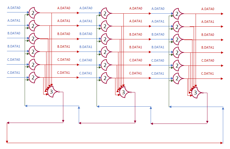
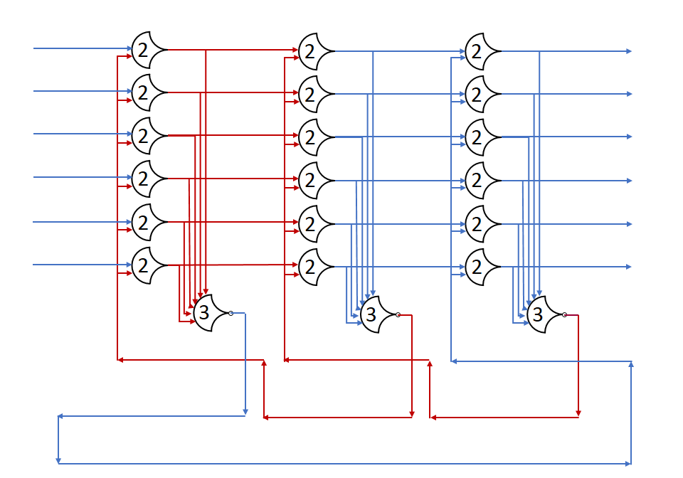
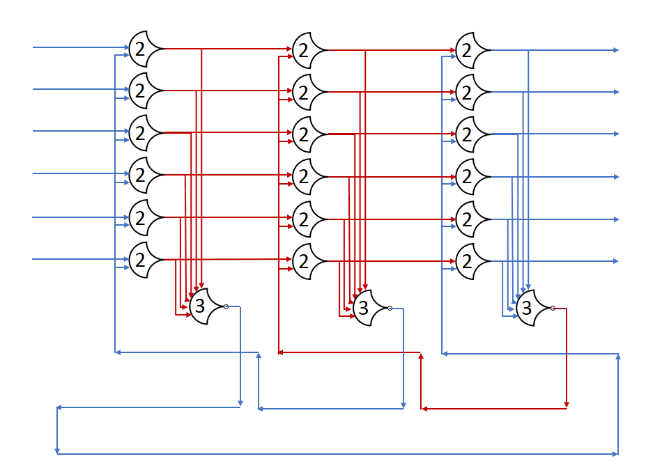
Minimized Pipeline

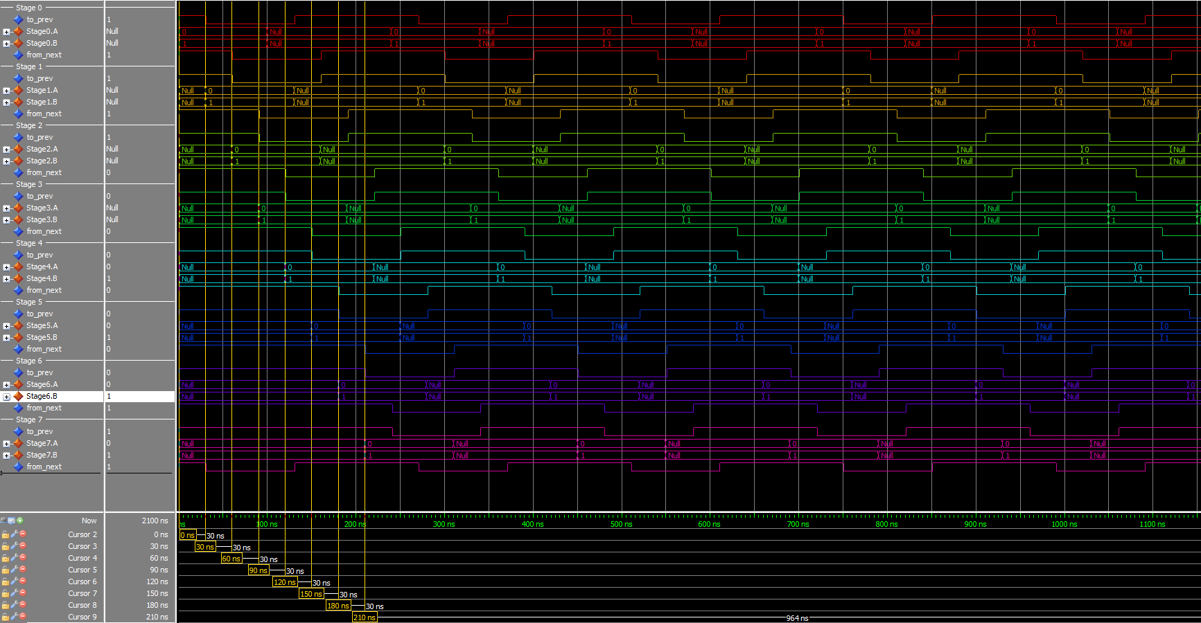
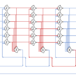
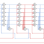
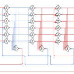
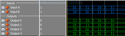
By our formula above, we need 4+1=5 stages. The initial state:

5-stage-pipeline.png

By putting the value of 0 in the first DATA state, and 1 in the second state, we can track when the ring completes a cycle. Throughput is 2/t_complete (two DATA states per trip around the ring) and latency is t_complete.
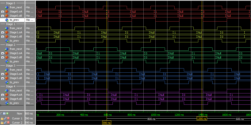
5-stage-4-state
5-stage ring with 2 DATA states and 2 NULL states
  • Throughput: 1/(400 ns) = 2.5 MHz
  • Latency: 800 ns

This experiment used the static_loop VHDL file, and a specific test script.

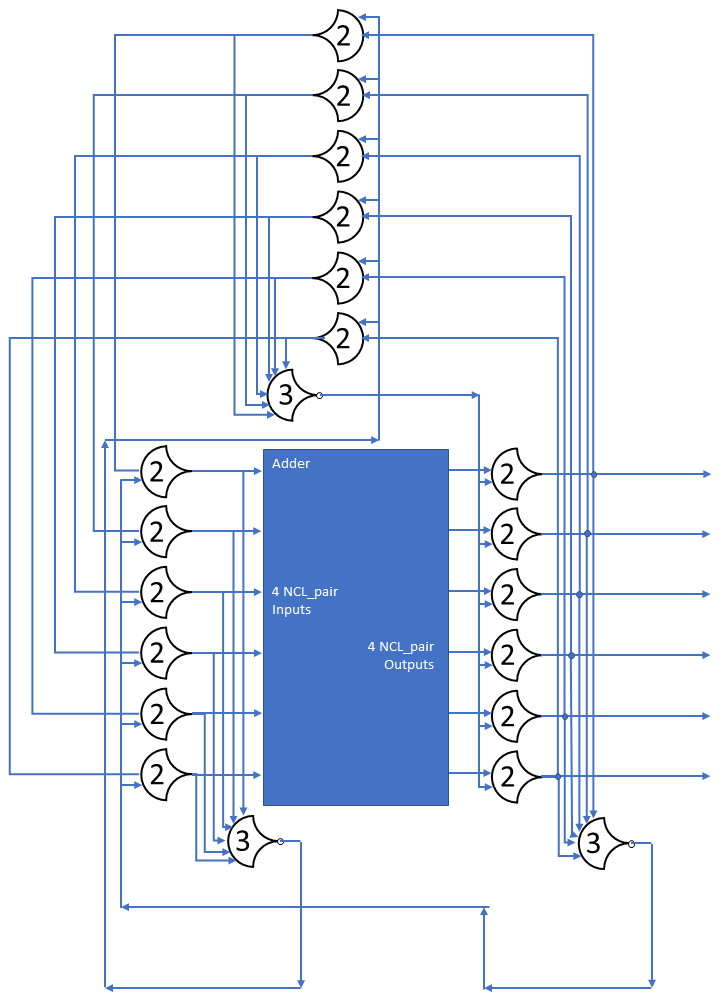
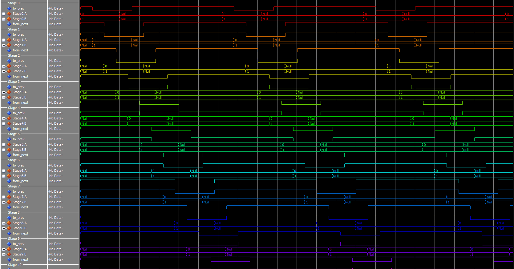
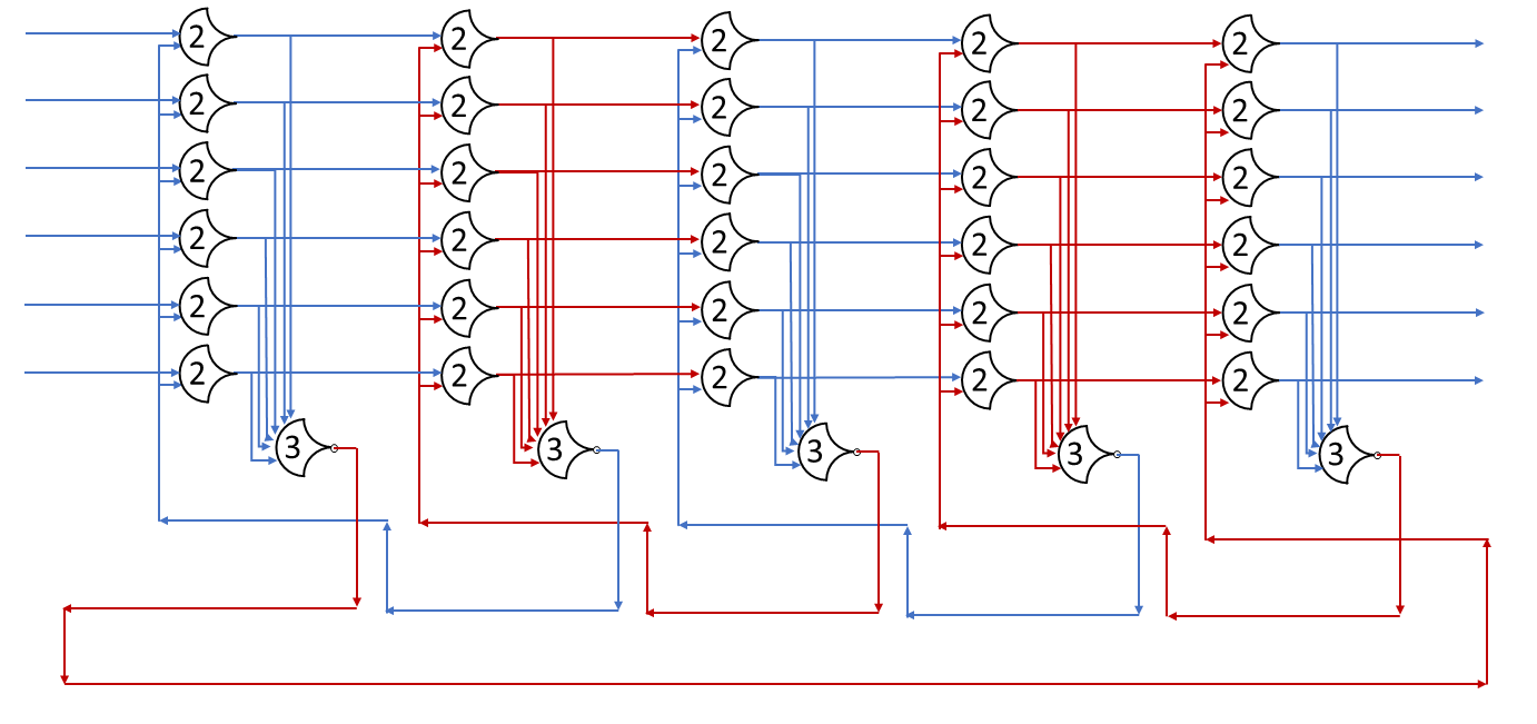
Throughput-Optimized Pipeline

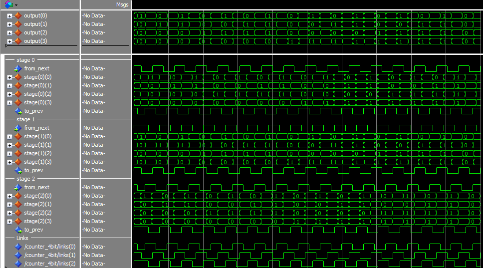
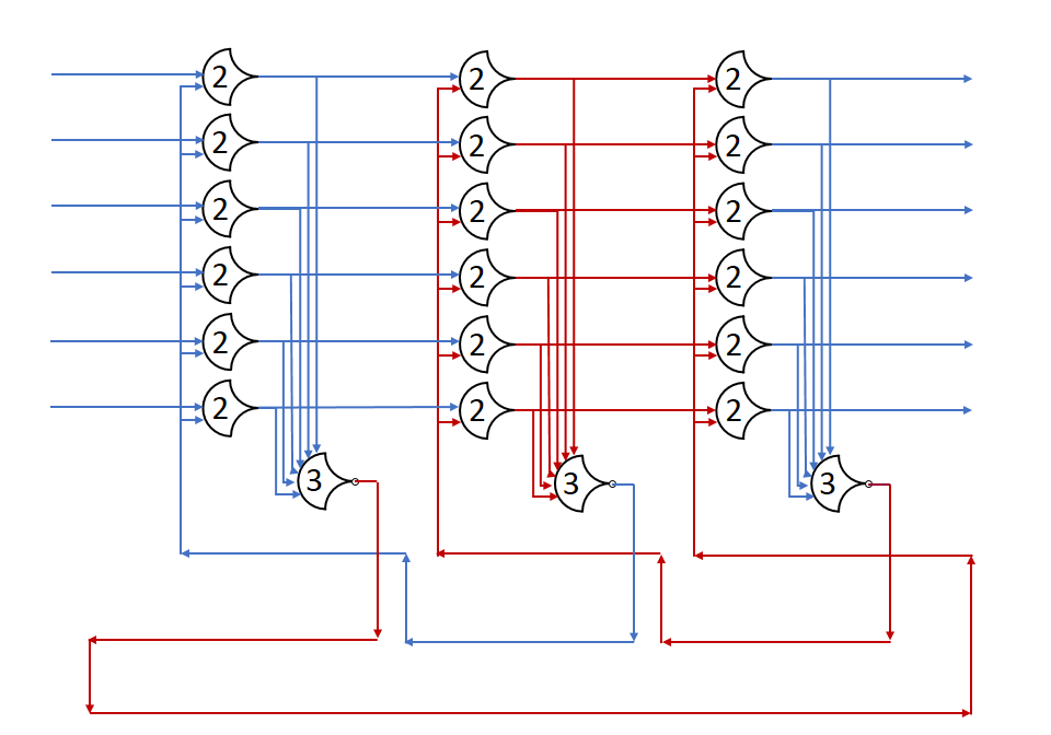
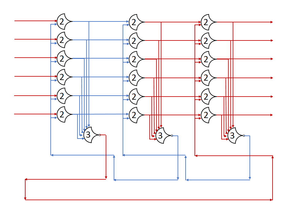
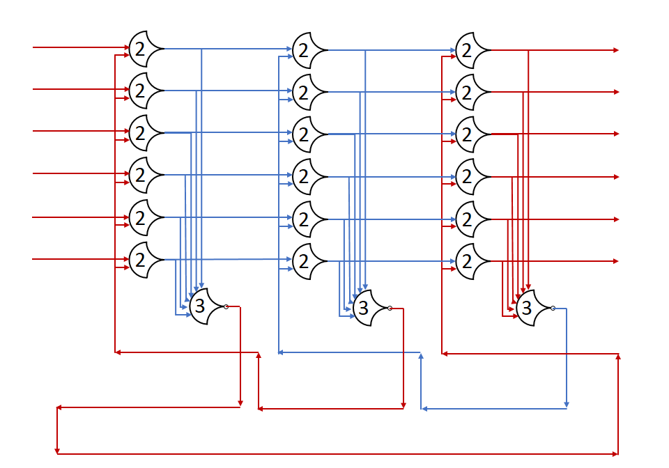
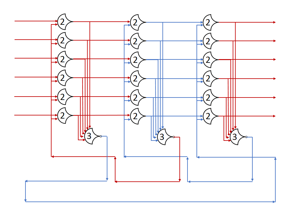
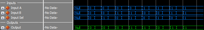
This version has 4+4=8 stages to go through, but all the states can move at the same time. Throughput should increase, but latency may increase as well. I’m not going to show the diagram because of size problems, but it’s a lot like the above, just with more stages.

Throughput and latency are calculated from the simulation, just as before. For optimal throughput and startup latency, arrange the states in pairs – 2 DATA, then 2 NULL, then 2 DATA, … – this increases the number of Advancement options at the start to the maximum: NumStates.
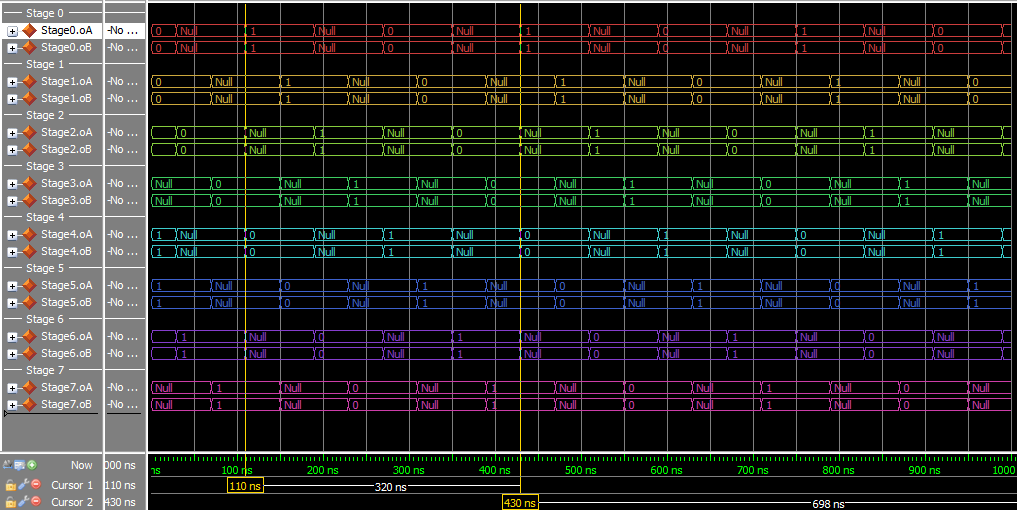
8-stage-4-state
An 8-stage ring with 2 DATA states and 2 NULL states
  • Throughput: 1/(160 ns) = 6.25 MHz
  • Latency: 320 ns

This experiment used the static_loop VHDL file, and a specific test script.

Results

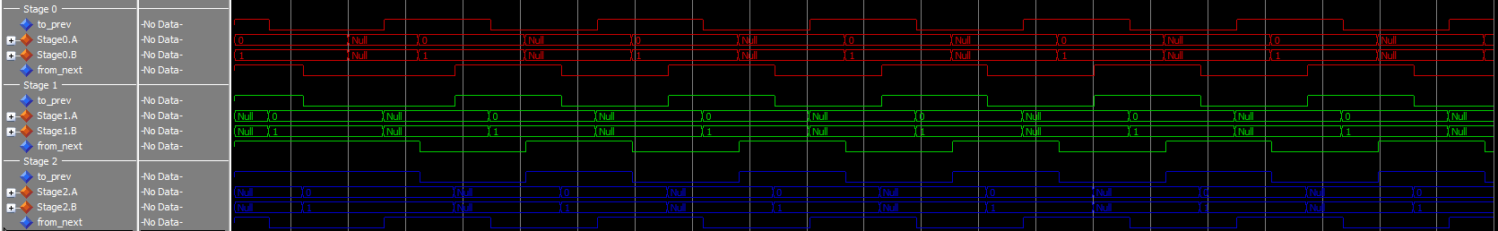
It looks like the throughput-optimized pipeline indeed has a higher throughput: By adding 3 states, we were able to more than double the efficiency of the ring, if you look at the simulation waveforms, in the first one only one stage is transitioning at a time. In the second, 4 stages are transitioning at a time. The second (faster) version uses 8/5 the resources though, so the decision on how many stages to use depends on available die space as well. In simulation, we don’t have to worry about this.

Commits: 997b4bb, be37b7f, 20ddd65

Running my Designs/Tests

To run a test, please make sure you have the correct version of the repository. Most posts that involve VHDL source will mention a commit, with a link (if you find a post that should have one and it doesn’t, please let me know).

Open ModelSim

If you are a student, you can get the PE student version from Mentor here, or your university might have it in a computer lab

Open the project file (NCL Gates/NCL Gates.mpf) with ModelSim.

Type source scripts/tests/[testname].tcl where [testname] is the name of a test file in the scripts/tests/ folder.

My tests should compile the dependencies automatically, but I might have missed something at some point, so let me know if it doesn’t work.

4-Bit Counter

Now that we’ve covered making data flow in circles, let’s use that to make a closed-system 4-bit counter. The module will have 4 state bits and 5 outputs (sum & carry out). To do this we’ll need an adder. I have a ripple carry NCL adder here.

We are going to put the adder between two registers, with a third register going back to hold the state during the NULL wavefront.

4bit_counter

The circuit shown is for a 3-bit adder, just to save space. The concept is the same, just add a bit to each register. Additionally, the adder has a static “0001” input for the B operand, which clears to NULL when the A input goes to NULL, this could be synthesized as the lines that get asserted being gated with TH22 gates with the watcher gate output (non-inverted) being the second input.

The source for this can be found here, and the simulation script here. Below is a simulation of the circuit. The first rows are the output, the next 3 sets are the registers.

Capture

The output cycles from 0 to 15, then resets to 0. During the reset cycle, the Adder’s Carry Out bit is set.

Conclusion

This is a pretty simple sequential circuit, but it demonstrates how to properly feed back the data. The third register is needed because the ‘business logic’ has to be able to go to NULL, without the whole thing losing state.

Commit: 5854b0c

VHDL source, Test Script

N-bit Ripple Carry Adder

Register Ring

I want to start in on some sequential logic. We have a few combinational modules that we can build on already, so the est thing would be to make a sequential-only circuit. Once we’ve clarified how the concept works, we can add in combinational logic in.

By ‘sequential-only’, I am referring to a setup with only registers, it just passes it’s initial input in a loop forever, not changing it. I’m hoping it’ll help me with the concept a bit more, and flush out any issues with the registers.

Here’s a diagram of a three stage loop, just imagine the outputs loop back (drawing it would be messy):

ring.png

Runtime Behavior

Let the initial state of the first stage’s outputs be DATA, with the first stage requesting NULL. The second and third stages are outputting NULL, and requesting DATA. Now let red be DATA, and blue be NULL.Slide1

After the gate delay for the register, the DATA wave is passed, and a request for NULL is sent back.

Slide2Slide3Slide4Slide5Slide6

And, we’re back where we started

Slide7

The ring will continue indefinitely. The VHDL source is available here, though without the test script, all stages remain at NULL, requesting DATA. I simulated this, and t turns out that it’s harder to see the pattern in graph form. To make things easier, I raised the number of stages.

Capture

At 8 stages, I start to be able to see it clearly as distinct wavefronts going through the pipeline. To make it really obvious, ramp it up to 12.

Capture

Not all stages shown.

And finally, if set at three, the pattern is harder to see, but it’s there. In the 3-stage case, the time spent requesting NULL and requesting DATA is the same for each stage.

Capture

If you use 2 stages, the system locks. A slideshow version of the ring pictures from above. As you can see, the transition to NULL only occurs while there are 2 DATA stages, and the transition to DATA only occurs while there are 2 NULL stages. This is so that no wavefront is ever ‘overwritten’. The second instance of that state saves the value.

NCL Decoder Implementation

Design Recap

The circuit diagram of the decoder:

DMUX2

This decoder will be generic, and be implemented much like the MUX.

Implementation

Each row will be generated based on it’s index. For each input:

  • If it is set:
    • Use DATA0 for the DATA0 of that case’s output
    • Use DATA1 for the DATA1 of that case’s output
  • If it is clear:
    • Use DATA1 for the DATA0 of that case’s output
    • Use DATA0 for the DATA1 of that case’s output

The DATA0 output sets are combined with a THN1, and the DATA1 outputs are combined with a THNN:

Rows: for i in 0 to NumOutputs - 1 generate
  cntlBits: for iBit in 0 to NumInputs - 1 generate
    Cntl0Selection: if (to_signed(2**iBit, NumInputs+1) and to_signed(i, NumInputs+1)) = 0 generate
      Gate0Inputs(i)(iBit) <= inputs(iBit).DATA1;
      Gate1Inputs(i)(iBit) <= inputs(iBit).DATA0;
    end generate;

    Cntl1Selection: if (to_signed(2**iBit, NumInputs+1) and to_signed(i, NumInputs+1)) > 0 generate
      Gate0Inputs(i)(iBit) <= inputs(iBit).DATA0;
      Gate1Inputs(i)(iBit) <= inputs(iBit).DATA1;
    end generate;
  end generate;

  Gate0: THmn
    generic map(N => NumInputs, M => 1)
    port map(inputs => Gate0Inputs(i),
             output => outputs(i).DATA0);
  Gate1: THmn
    generic map(N => NumInputs, M => NumInputs)
    port map(inputs => Gate1Inputs(i),
             output => outputs(i).DATA1);
end generate;

This assigns input cases to the gates. If any non-selected values are asserted, then the DATA0 line of that case is asserted.

Adding the declarations around it:

library ieee;
use ieee.std_logic_1164.all;
use work.ncl.all;
use ieee.numeric_std.all;

entity Decoder is
  generic(NumInputs : integer := 2);
  port(inputs  : in  ncl_pair_vector(0 to NumInputs-1);
       outputs : out ncl_pair_vector(0 to (2**NumInputs)-1));
end entity Decoder;

architecture structural of Decoder is
  constant NumOutputs : integer := 2 ** NumInputs;

  type GateInputs is array (integer range <>) of std_logic_vector(0 to NumInputs - 1);
  signal Gate0Inputs : GateInputs(0 to NumOutputs-1);
  signal Gate1Inputs : GateInputs(0 to NumOutputs-1);
begin
  Rows: for i in 0 to NumOutputs - 1 generate
    cntlBits: for iBit in 0 to NumInputs - 1 generate
      Cntl0Selection: if (to_signed(2**iBit, NumInputs+1) and to_signed(i, NumInputs+1)) = 0 generate
        Gate0Inputs(i)(iBit) <= inputs(iBit).DATA1;
        Gate1Inputs(i)(iBit) <= inputs(iBit).DATA0;
      end generate;

      Cntl1Selection: if (to_signed(2**iBit, NumInputs+1) and to_signed(i, NumInputs+1)) > 0 generate
        Gate0Inputs(i)(iBit) <= inputs(iBit).DATA0;
        Gate1Inputs(i)(iBit) <= inputs(iBit).DATA1;
      end generate;
    end generate;

    Gate0: THmn
             generic map(N => NumInputs, M => 1)
             port map(inputs => Gate0Inputs(i),
                      output => outputs(i).DATA0);
    Gate1: THmn
             generic map(N => NumInputs, M => NumInputs)
             port map(inputs => Gate1Inputs(i),
                      output => outputs(i).DATA1);
  end generate;
end structural;

Testing

I tested it for 2 inputs, to make sure the generics build correctly. The outputs do not go through all combinations, since only one is allowed to be DATA1 at a time. Here’s the test script

Capture

Commit: a58ee22

NCL Decoder Design

Theory

The decoder is like a backwards multiplexer, it uses the selector bits to output a DATA 1 on a single output, and DATA 0 on the others. This can be used to enable one of many modules, or just to change encoding from binary to one-hot.

Design

If you remember how we made the MUX module, we had a loop that generated a set of selector lines (DATA0 or DATA1 from each selector input) for each case. We will re-use this, but we will generate a TRUE and FALSE signal for each case (DATA0 and DATA1 of the corresponding output). The TRUE gate for each case will be a THNN, and the FALSE gate will be a TH1N. Here is what a Decoder2 module would look like:

DMUX2

The inputs to the TH1N gates (FALSE) are the opposing rails to the THNN gate of the same case.

  • CaseTrue='All bits for this case set'
  • CaseFalse='Any other bit set'

Any NULL input produces some NULL output: The THNN gates (TRUE) can’t set because they will always be missing an input, and for any particular input (missing a bit) there are two possible outputs: one with the bit set and one with it clear; these FALSE outputs will remain off as they need the DATA0 and DATA1 respectively from the missing input.

The decoder is actually a fairly simple gate. It is possible to split the DMUX into two parts: DMUX1, and DMUX0. These components would output the DATA1 and DATA0 lines respectively. They are not valid as complete NCL components, but they are useful: You can make a MUX by using a DMUX1 and 2*NumOptions TH22 gates. This might be especially useful when making a MUX that takes in multi-bit options. A single DMUX1 would be used to generate the control signals, and each signal of each bit of each option would be gated with the TH22 gates.

Input Completeness

So, I have been doing more reading, and I found a concept that I think I glossed over up to this point. Input Completeness is the condition that the output should not change until all inputs are available. This must hold for both NULL->DATA and DATA->NULL wavefronts. I don’t actually understand why this is necessary yet.

I had vaguely considered the concept as weather or not internal lines would ever toggle more than once during a single data cycle, but I thought that since all data was expressed by asserted lines, a system couldn’t toggle as long as there were no inverters. Even if there was feedback, none of the gates use compliments of inputs, so adding more inputs either sets the gate, or leaves it alone. There is no way to clear a set line, without clearing an input. I will look into the reasons this condition is necessary at some point.

Quick thing: I will be using the term CSOP a bunch. It means Canonical Sum-of-Product. This is the version of the equation that has all of the truth table rows brought out separately. Even if the function can be optimized to eliminate a variable from a term or two, that would violate the rules of CSOP.

The NULL->DATA Wavefront

If the circuit is initially NULL (inputs, outputs, internals) then the outputs cannot change until all inputs are DATA. The simplest way to do this is to use the CSOP implementation. With CSOP, every input is used in one of the AND-Plane gates (either as DATA0 or DATA1). As such, none of the AND-Plane gates can trigger until all of the inputs have values.

The AND-Plane is the column of THNN gates that all the inputs tie into (all possible combinations of input DATA values).

The DATA->NULL Wavefront

The DATA->NULL transition for any individual gate is held until all its inputs go to NULL. As such, once an output is set, it won’t clear until its inputs clear. Unfortunately that only applies to the inputs involved in setting the output; in CSOP, again, this is all of them. If the output is not constructed with CSOP, then in some cases, some inputs won’t affect the outputs (think the unselected inputs of a MUX).

Solutions

It is not necessary to implement the function with CSOP, you can take the logic function and add (A.0+A.1) to the product terms that are missing A, for example. The function can then be simplified/expanded from there. This is described some here on page 17 (section 3.1):

 Smith, Scott C., and Jia Di. Designing Asynchronous Circuits Using NULL Convention Logic (NCL) Scott C. Smith and Jia Di. San Rafael, Calif.]: Morgan & Claypool, 2009. Print. Synthesis Lectures on Digital Circuits and Systems #23.

I haven’t found a openly available source for this, if you are a student, check your university’s library website. If you do find a source, comment it.

NCL Multiplexer Implementation

Design RecapMUX4

4-Option Example

for Case in 0 to N-1
  [build CaseBits with DATA0's and DATA1's]
  -- CaseBits is a concatenated signal from the iSelector input
  Selectors(Case) <= THNN(CaseBits)

  GatedCase0 <= TH22(Selectors(Case), iOptions(Case).DATA0)
  GatedCase1 <= TH22(Selectors(Case), iOptions(Case).DATA1)
next Case

output.DATA0 <= TH1N(Gated00, Gated10, Gated20, Gated30, ...)
output.DATA1 <= TH1N(Gated01, Gated11, Gated21, Gated31, ...)

Generic pseudo-VHDL

Implementation

Remember the Full Adder‘s un-optimized version? If you look at the implementation, you’ll see a chunk of code at the top that generates one-hot encoding of all cases. We are going to use that for our internal Selectors signal:

cases: for case in 0 to NumOptions generate
  bits: for ibit in 0 to NumSelectors-1 generate

    Input0Selection: if (to_unsigned(2**iBit, 3) and to_unsigned(case, 3)) = 0 generate
      selectorInputs(case)(iBit) <= iOptions(case).DATA0;
    end generate;

    Input1Selection: if (to_unsigned(2**iBit, 3) and to_unsigned(case, 3)) > 0 generate
      selectorInputs(case)(iBit) <= iOptions(case).DATA1;
    end generate;
  end generate;

  CaseSelectorGate: THmn
    generic map(M => NumSelectors, N => NumSelectors)
    port map(inputs => selectorInputs(case),
             output => Selectors(case));

 end generate;

Next, we need to gate the two lines (DATA0 and DATA1) for each option, which will NULL them if they are not the selected signal:

cases: for case in 0 to NumOptions generate
  bits: for ibit in 0 to NumSelectors-1 generate

    Input0Selection: if (to_unsigned(2**iBit, 3) and to_unsigned(case, 3)) = 0 generate
      selectorInputs(case)(iBit) <= iOptions(case).DATA0;
    end generate;

    Input1Selection: if (to_unsigned(2**iBit, 3) and to_unsigned(case, 3)) > 0 generate
      selectorInputs(case)(iBit) <= iOptions(case).DATA1;
    end generate;
  end generate;

  CaseSelectorGate: THmn
    generic map(M => NumSelectors, N => NumSelectors)
    port map(inputs => selectorInputs(case),
             output => Selectors(case));

  Gated0: THmn
    generic map(M => 2, N => 2)
    port map(inputs(0) => Selectors(case),
             inputs(1) => iOptions(case).DATA0,
             output => GatedOptions0(case));

  Gated1: THmn
    generic map(M => 2, N => 2)
    port map(inputs(0) => Selectors(case),
             inputs(1) => iOptions(case).DATA1,
             output => GatedOptions1(case));

 end generate;

Finally, take all those gated options and or the signals together, so whichever one is selected will drive the line to a 1 if it is set:

cases: for case in 0 to NumOptions generate
  bits: for ibit in 0 to NumSelectors-1 generate

    Input0Selection: if (to_unsigned(2**iBit, 3) and to_unsigned(case, 3)) = 0 generate
      selectorInputs(case)(iBit) <= iOptions(case).DATA0;
    end generate;

    Input1Selection: if (to_unsigned(2**iBit, 3) and to_unsigned(case, 3)) > 0 generate
      selectorInputs(case)(iBit) <= iOptions(case).DATA1;
    end generate;
  end generate;

  CaseSelectorGate: THmn
    generic map(M => NumSelectors, N => NumSelectors)
    port map(inputs => selectorInputs(case),
             output => Selectors(case));

  Gated0: THmn
    generic map(M => 2, N => 2)
    port map(inputs(0) => Selectors(case),
             inputs(1) => iOptions(case).DATA0,
             output => GatedOptions0(case));

  Gated1: THmn
    generic map(M => 2, N => 2)
    port map(inputs(0) => Selectors(case),
             inputs(1) => iOptions(case).DATA1,
             output => GatedOptions1(case));

 end generate;

o0: THmn
  generic map(M => 1, N => NumOptions)
  port map(inputs(0) => GatedOptions0(case),
           output => output.DATA0);

o1: THmn
  generic map(M => 1, N => NumOptions)
  port map(inputs => GatedOptions1(case),
           output => output.DATA1);

That’s all the logic then, but we need to add the wrapping structures (entity declaration, architecture declaration, and internal signal declarations). This module will have one generic parameter (NumOptions), and a constant based on it (NumSelectors). The width of the iSelector input will be the log of the number of options:

entity MUX is
  generic(NumOptions : integer := 2);
  port (iSelector : in ncl_pair_vector(0 to clog2(NumOptions)-1);
        iOptions  : in ncl_pair_vector(0 to NumOptions1-);
        output   : out ncl_pair);
end MUX;

architecture structural of MUX is
  constant NumSelectors : integer := clog2(NumOptions);
  signal Selectors : std_logic_vector(0 to NumOptions-1);
  signal GatedOptions0 : std_logic_vector(0 to NumOptions-1);
  signal GatedOptions1 : std_logic_vector(0 to NumOptions-1);

  type SelectorData is array (integer range ) of std_logic_vector(0 to NumSelectors-1);
  signal selectorInputs : SelectorData(0 to NumOptions-1);
begin
  -- [This part is the same as before]
  
  cases: for case in 0 to NumOptions generate
    bits: for ibit in 0 to NumSelectors-1 generate

      Input0Selection: if (to_unsigned(2**iBit, 3) and to_unsigned(case, 3)) = 0 generate
        selectorInputs(case)(iBit) <= iOptions(case).DATA0;
      end generate;

      Input1Selection: if (to_unsigned(2**iBit, 3) and to_unsigned(case, 3)) > 0 generate
        selectorInputs(case)(iBit) <= iOptions(case).DATA1;
      end generate;

      CaseSelectorGate: THmn
        generic map(M => NumSelectors, N => NumSelectors)
        port map(inputs => selectorInputs(case),
                 output => Selectors(case));
    Gated0: THmn
      generic map(M => 2, N => 2)
      port map(inputs(0) => Selectors(case),
               inputs(1) => iOptions(case).DATA0,
               output => GatedOptions0(case));

    Gated1: THmn
      generic map(M => 2, N => 2)
      port map(inputs(0) => Selectors(case),
               inputs(1) => iOptions(case).DATA1,
               output => GatedOptions1(case));

    end generate;

  o0: THmn
    generic map(M => 1, N => NumOptions)
    port map(inputs(0) => GatedOptions0(case),
             output => output.DATA0);

  o1: THmn
    generic map(M => 1, N => NumOptions)
    port map(inputs => GatedOptions1(case),
             output => output.DATA1);

end structural;

Testing

I am testing this module with 2 inputs for now; in theory it scales, but at some point I should add a 4-option test, and maybe a 5 to see how it does with non-power of 2 values. The test script goes through the inputs options and tests that they output correctly.

When I first ran this, I had an error where the outputs indexing was in the wrong order. I had the part of the code near the top messed up to use iSelectors(case).DATA0 instead of DATA1 and vice versa.

Capture

Commit: b35b729

NCL Multiplexer Design

Theory

Multiplexers are components that let you switch between different options for a signal. They take in some number of option values (usually a power of 2) and a selector. Each data value of the selector corresponds to a particular input, which is fed to the output.

output = iOptions(iSelector)

If there are 2 options (the most basic MUX) then the selector is 1 bit. If there are 3 or 4 options 2 bits are needed, and so on.

Design

This time we’re going to go about this in a more intuitive, less rigorous, manner. Let’s consider each ‘row’ separately, each row will correspond to one input option (both *.0 and *.1). For each of these rows, we’ll generate a gating signal from the iSelector bits. This gating signal will be used by two TH22 gates to clear all but the selected signals.

This is very much like having 2 MUXes, one for the *.1s and one for the *.0‘s.

We’ll be reusing some code from the FullAdder implementation to get the selectors (one wire per input case); each of these will gate the DATA0 and DATA1 lines of the respective input option. The gated values will then be combined with a TH1n gate. An example 4-option case:

Case0 <= TH22(iSel(0).DATA0, iSel(1).DATA0)
Case1 <= TH22(iSel(0).DATA1, iSel(1).DATA0)
Case2 <= TH22(iSel(0).DATA0, iSel(1).DATA1)
Case3 <= TH22(iSel(0).DATA1, iSel(1).DATA1)

GatedA0 <= TH22(iOptions(0).DATA0, Case0)
GatedA1 <= TH22(iOptions(0).DATA1, Case0)

GatedB0 <= TH22(iOptions(1).DATA0, Case1)
GatedB1 <= TH22(iOptions(1).DATA1, Case1)

GatedC0 <= TH22(iOptions(2).DATA0, Case2)
GatedC1 <= TH22(iOptions(2).DATA1, Case2)

GatedD0 <= TH22(iOptions(3).DATA0, Case3)
GatedD1 <= TH22(iOptions(3).DATA1, Case3)

output.DATA0 <= TH14(GatedA0, GatedB0, GatedC0, GatedD0)
output.DATA1 <= TH14(GatedA1, GatedB1, GatedC1, GatedD1)

mux42.png

That’s a bit repetitive, let’s make it a little more general. The design involves some ‘magic’ parts because they are more of an implementation detail really.

for Case in 0 to N-1
  [build CaseBits with DATA0's and DATA1's]
      -- CaseBits is a concatenated signal from the iSelector input
  Selectors(Case) <= THNN(CaseBits)

  GatedCase0 <= TH22(Selectors(Case), iOptions(Case).DATA0)
  GatedCase1 <= TH22(Selectors(Case), iOptions(Case).DATA1)
next Case

output.DATA0 <= TH1N(Gated00, Gated10, Gated20, Gated30, ...)
output.DATA1 <= TH1N(Gated01, Gated11, Gated21, Gated31, ...)

Each row generates a selector, gates the option values, and passes them to the output. Any un-selected inputs are NULLed out (Gated#0 and GATED#1 both go to 0) leaving only the selected input to pass through the TH1N gates.

Using an NCL Register

In this post, I described what a NCL register is. I wanted to get a more practical understanding of what the register does and how different pipeline stages interact. To facilitate this, I put the Full Adder between two registers, with their control signals linked:

pipelinedadder.png

In this setup, both registers start with NULL, requesting DATA.

  1. When DATA is fed to the first register, it immediately passes it on to the adder and requests NULL
  2. Once the Adder completes, the second register saves the DATA to the outputs and requests NULL.

The same sequence repeats with the NULL wavefront, then back to DATA, and so on…

We’ve already tested the Adder, but we want to make sure the system works, so we make a separate test for this unit (VHDL source, TCL test script). This test doesn’t actually verify the results of the computation as we already checked the adder. Essentially, if it runs, the pipelining  worked. If it hangs, then something is wrong and wavefronts are not propagating through the circuit.

Pipelined Adder tests

In theory, a loop with 3 registers can be made, but in this case, if the outputs feed back, the result will degrade to 1 eventually, or stay at 0. I may make a 2-bit counter or something in a while.

Commit: 40d96b8