Shifter

Theory

A Shifter takes an array of bits, and shifts them right of left. Numerically, this is like multiplying or dividing by 2 (in the case of binary numbers). Some examples:

Direction Input Shift Amount Output
Right 001001  1 000100
Left 001001  1 010010
Right 001001  2 000010
Left 001001  3 001000

This could be applied to non-binary variables as well (like 3-rail signals) but the exact meaning will be different. There are a few ‘extensions’ to this behavior I’d like to add:

  • Rotation
  • Arithmetic shifting

Rotation allows the bits shifted out one end to be shifted back in the other:

Direction Input Output
Right 1001 1100
Left 1001 0011

Arithmetic shifting treats the shift as a mathematical operation and preserves the sign of the number. It is only valid for right shifts.

Direction Input Output
Right 100(-4) 110(-2)
Right 110(-2) 111(-1)

The sign of a number is represented by leading 1’s in the MSB, so an arithmetic right shift adds 1’s into the leftmost bits, if the number was negative. This is accomplished by shifting in the MSB.
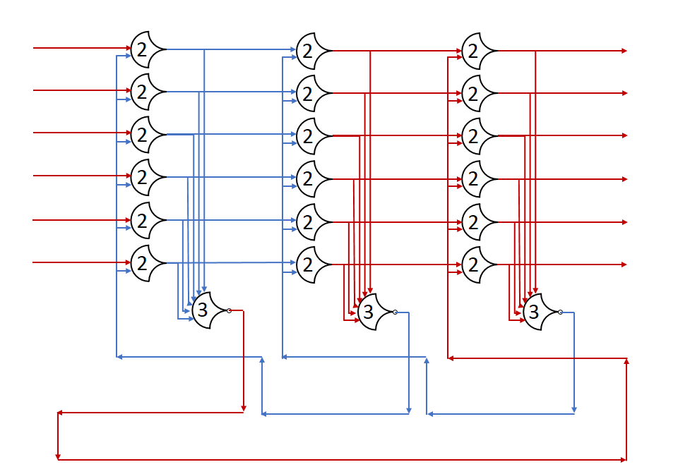
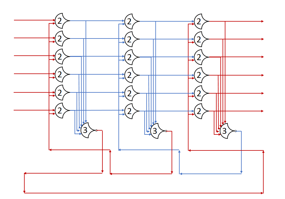
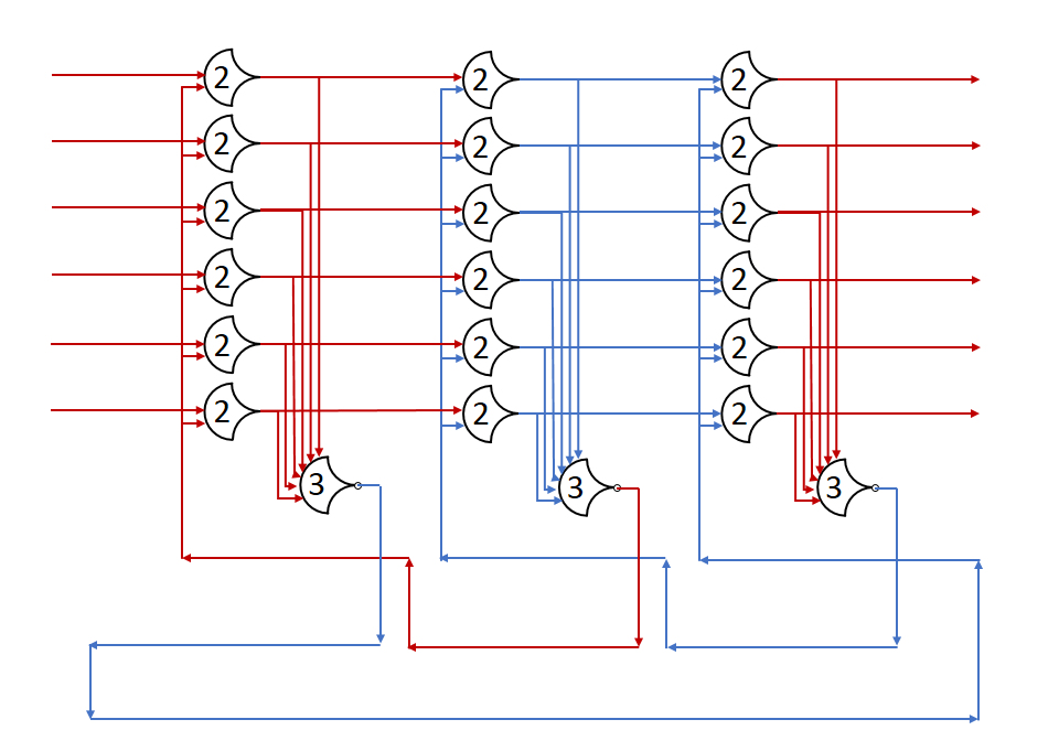
Design

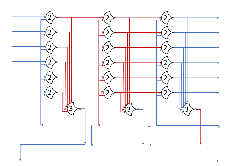
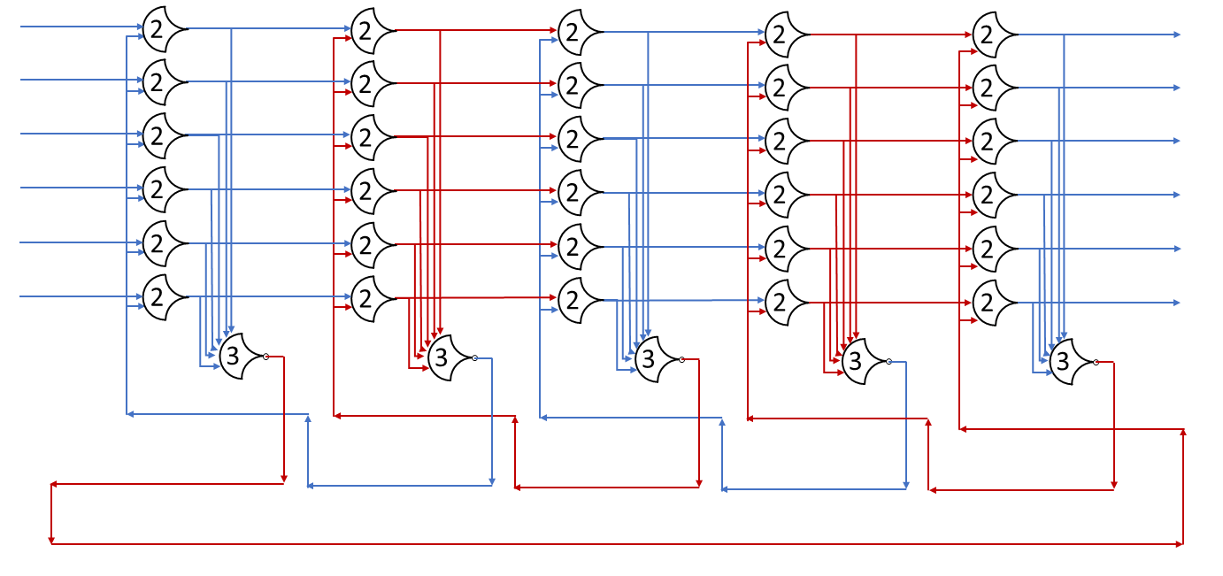
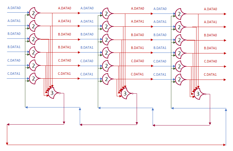
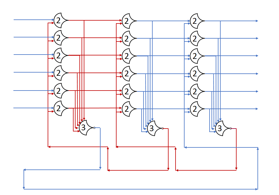
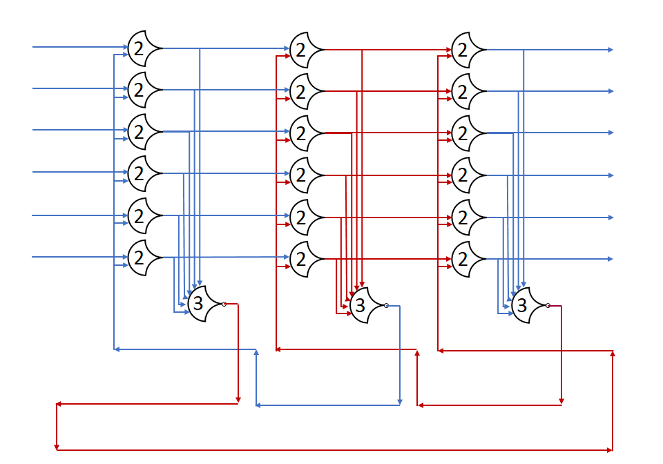
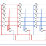
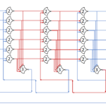
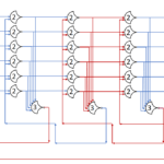
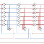
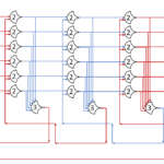
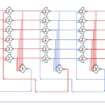
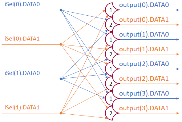
Each shift_amount bit corresponds to a shift of 2^n, where n is the index of the bit. Each constant-size shift can be accomplished with only wiring. As my CprE 381 professor always said, if you have two possible values, the easiest way to pick one is a MUX. So, each shift_amount bit will choose between an unshifted, or 2^n shifted value. By connecting these in layers, we get a shift of any size.

BasicShifter

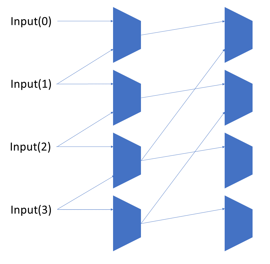
The un-supplied inputs are 0’s. The first column is controlled by shift_amount(0), the second column is controlled by shift_amount(1).

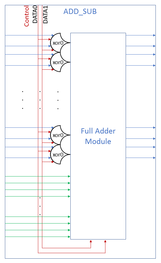
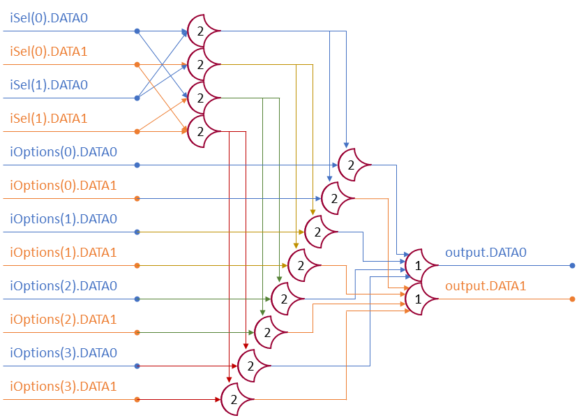
To change the direction, we add a mux at the beginning that selects a reversed version of the input, let the shifter shift that, then un-reverse it at the end.

To add rotations, we add another input to the MUX’s at the bottom that feeds back from the top, so that the ‘lost’ bits are shifted back in.

basicshifter1.png

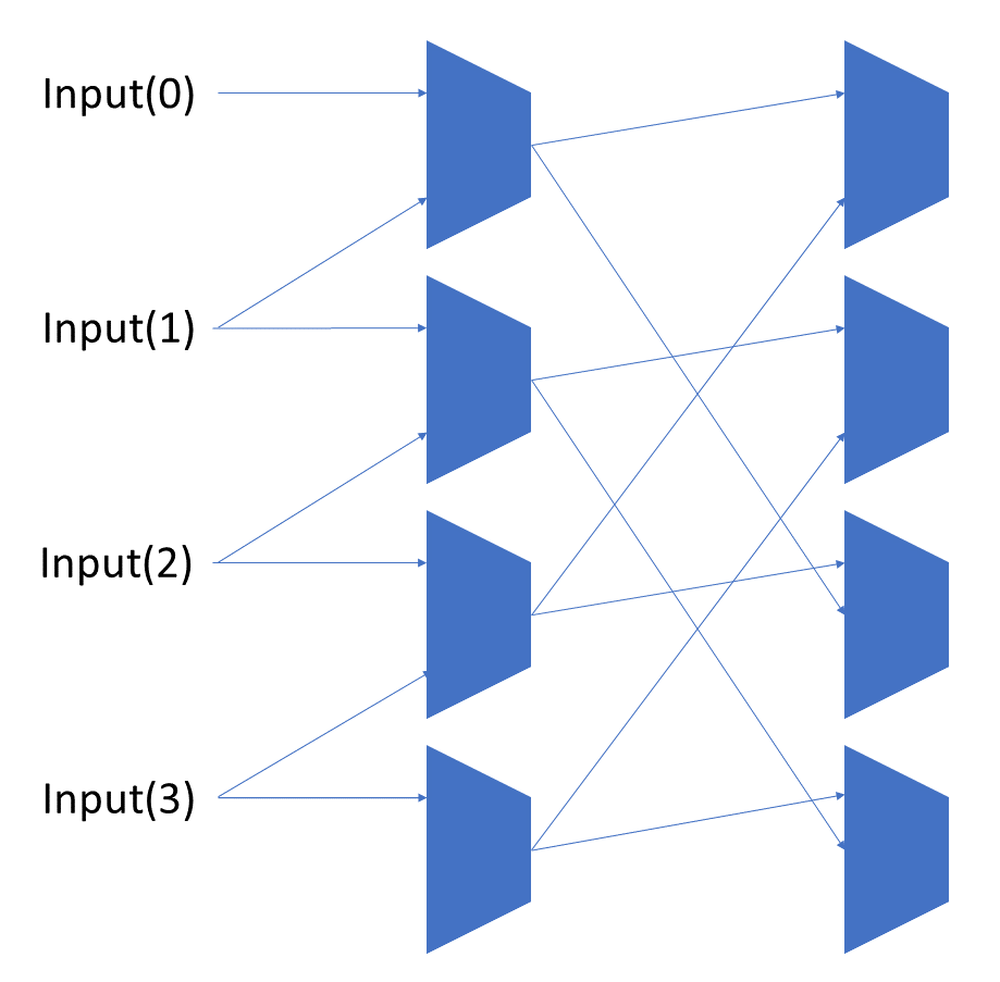
To add arithmetic operations, the unassigned inputs in the lower MUX’s are changed from 0 to the MSB of the input. This signal is constant across all the MUX’s it is applied to, so it is generated with a single MUX. On a left shift, the shifted-in value must be 0, so the MUX can only output the MSB when a right arithmetic shift is selected.
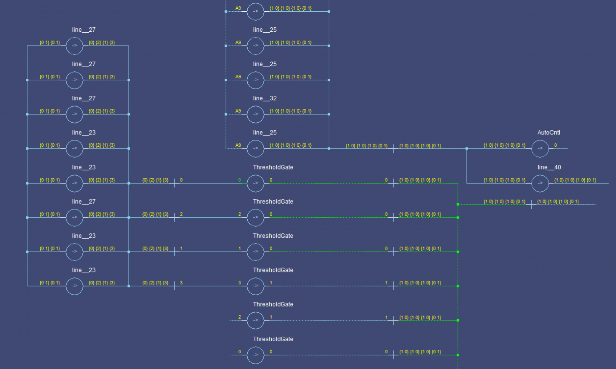
Implementation

the VHDL source, using generics to make it work for any number of inputs (even non-powers of 2, btw):

library ieee;
use work.ncl.all;
use ieee.std_logic_1164.all;

entity Shifter is
  generic(NumInputs : integer := 2);
  port(inputs       : in ncl_pair_vector(0 to NumInputs - 1);
       shift_amount : in ncl_pair_vector(0 to clog2(NumInputs) - 1);
       direction    : in ncl_pair;
       rotate       : in ncl_pair;
       logical      : in ncl_pair;
       output       : out ncl_pair_vector(0 to NumInputs - 1));
end Shifter;

architecture structural of Shifter is
  constant NumShiftAmountBits : integer := clog2(NumInputs);
  constant NumRows : integer := clog2(NumInputs);
  
  type RowSignals is array (integer range <>) of ncl_pair_vector(0 to NumInputs - 1);
  
  -- The shifted array at each stage of the shifter.
  signal rows : RowSignals(0 to NumRows);
  
  -- A generated value that is always DATA0 or NULL as appropriate
  signal zero_in : ncl_pair;
  
  -- The third input that is used for either logical or arithmetic operations.
  signal non_rotate_in : ncl_pair;

  signal input_reversed : ncl_pair_vector(0 to NumInputs - 1);
  signal output_reversed : ncl_pair_vector(0 to NumInputs - 1);

begin

  produceDATA0: THmn 
    generic map(M => 1, N => 2)
    port map(inputs(0) => inputs(0).DATA0,
             inputs(1) => inputs(0).DATA1,
             output => zero_in.DATA0);
  
  zero_in.DATA1 <= '0';   msb_in_mux: MUX     generic map(NumInputs => 4)
    port map(iOptions(0) => inputs(NumInputs-1),
             iOptions(1) => zero_in,
             iOptions(2) => zero_in,
             iOptions(3) => zero_in,
             iSel(0) => logical,
             iSel(1) => direction,
             output => non_rotate_in);

  in_bit_flipper: for i in 0 to NumInputs-1 generate
    input_reversed(i) <= inputs(NumInputs-1-i);     directionMux: MUX       generic map(NumInputs => 2)
      port map(iOptions(0) => inputs(i),
               iOptions(1) => input_reversed(i),
               iSel(0) => direction,
               output => rows(0)(i));
  end generate;

--  rows(0) <= inputs;

  rowsloop: for r in 0 to NumRows-1 generate
    columns: for c in 0 to NumInputs-1 generate
      ifstd: if (c + (2**r)) < NumInputs generate         multiplexer: MUX           generic map(NumInputs => 2)
          port map(iOptions(0) => rows(r)(c),
                   iOptions(1) => rows(r)(c + (2**r)),
                   iSel(0) => shift_amount(r),
                   output => rows(r+1)(c));

      end generate;

      ifwrp: if (c + (2**r)) >= NumInputs generate
        multiplexer: MUX
          generic map(NumInputs => 4)
          port map(iOptions(0) => rows(r)(c),
                   iOptions(1) => non_rotate_in,
                   iOptions(2) => rows(r)(c),
                   iOptions(3) => rows(r)((c+(2**r)) mod NumInputs),
                   iSel(0) => shift_amount(r),
                   iSel(1) => rotate,
                   output => rows(r+1)(c));

      end generate;
    end generate;
  end generate;

  out_bit_flipper: for i in 0 to NumInputs-1 generate
    output_reversed(i) <= rows(NumRows)(NumInputs - 1 - i);     outMux: MUX       generic map(NumInputs => 2)
      port map(iOptions(0) => rows(NumRows)(i),
               iOptions(1) => output_reversed(i),
               iSel(0) => direction,
               output => output(i));
  end generate;

end structural;

This code generates the necessary multiplexers for shifting the signal, flipping it at the input and output, and selecting how to handle the bits that can’t be shifted normally (because the source is out of range).
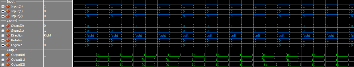
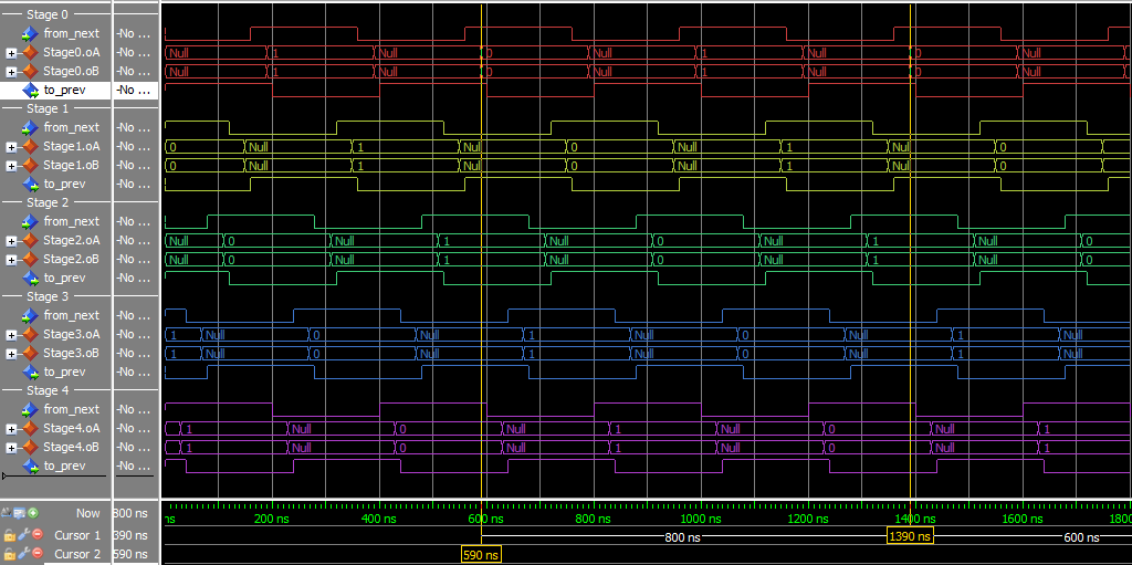
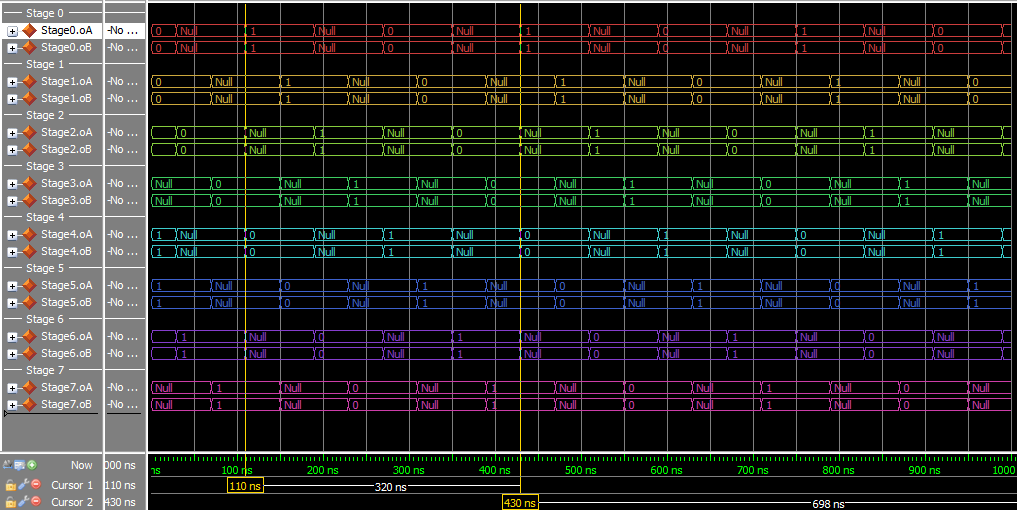
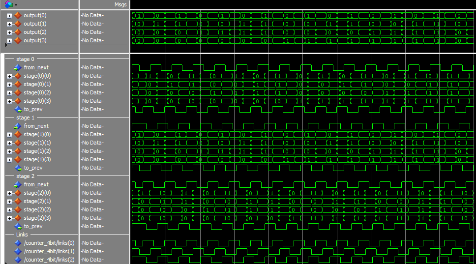
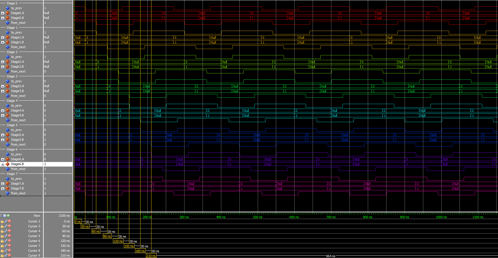
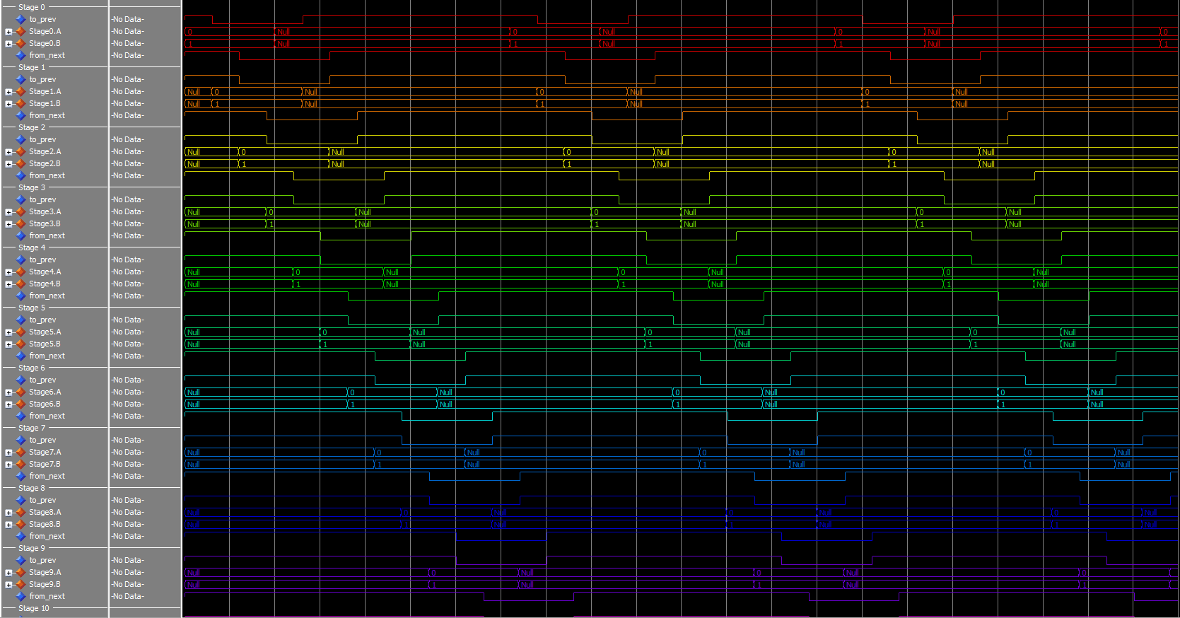
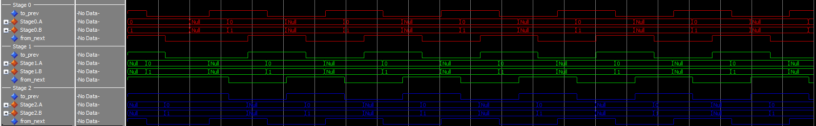
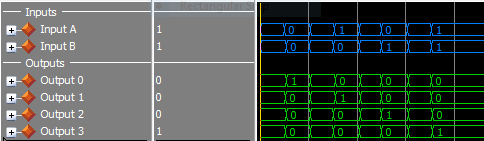
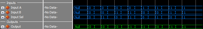
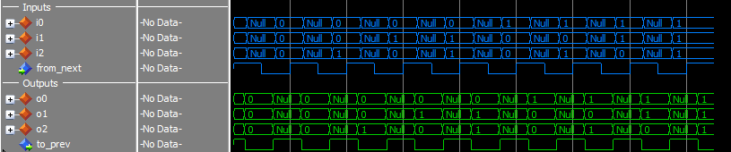
Testing

I made a simple test script to run through some cases. Everything seems to check out, here’s a sample:

Capture

Commit: 53d34cf, ef416eb

NCL Arithmetic Logic Unit – ADD/SUB

Theory

An arithmetic logic unit (ALU) is a component that performs operations on (usually) two or more sets of inputs, and outputs results. The operation performed is designated by an Operation signal.

Design

Our ALU will start simple, and we’ll add more operations over time. First, let’s build an add/sub unit. I already have an adder, which can be used to subtract by swapping some signals: In single-rail (standard) logic, to subtract instead of add, the second input to the adder is inverted and the carry bit is set – in NCL, we invert the input by swapping DATA0 and DATA1.

The swapper operates as the following equations

output.0 = input.0*swap.0 + input.1*swap.1
output.1 = input.1*swap.0 + input.0*swap.1

These can be implemented with THxor0 gates:

output.0 = THxor0(input.0, swap.0, input.1, swap.1)
output.1 = THxor0(input.1, swap.0, input.0, swap.1)

Our add/sub module will have these on every bit on input to the adder, with iC having the swap signal fed directly into it. Swap will be exposed in the component’s port as the add/subtract selector:

Add_Sub

Green is iA, blue is iB, and red is iC on the Adder. If Control is asserted (DATA1) iB will be inverted and the carry in will be asserted as well, resulting in subtraction.

This module actually fulfills the interface of an ALU by itself, it has data inputs, and a opcode. When we add more operations, we’ll wrap it all up in a ALU block and add a MUX.

Implementation

To implement this in VHDL, we need 1 Adder module and 2*N THxor0 gates:

use ieee.std_logic_1164.all;
use ieee.numeric_std.all;
use work.ncl.all;

entity AddSub is
  generic(NumBits : integer := 4);
  port(iA        : in ncl_pair_vector(0 to NumBits-1);
       iB        : in ncl_pair_vector(0 to NumBits-1);
       Operation : in ncl_pair;

       oS       : out ncl_pair_vector(0 to NumBits-1);
       oC       : out ncl_pair);
end AddSub;

architecture structural of AddSub is

  -- iB into adder, potentially inverted from entity input
  signal adder_iB : ncl_pair_vector(0 to NumBits-1);

begin

  plainAdder: Adder
    generic map(NumAdderBits => NumBits)
    port map(iC => Operation,
             iA => iA,
             iB => adder_iB,
             oS => oS,
             oC => oC);

  bits: for iBit in 0 to NumBits-1 generate

    inverter0: THxor0 -- DATA0, Potentially inverted
      port map(A => iB(iBit).DATA0,
               B => Operation.DATA0,
               C => iB(iBit).DATA1,
               D => Operation.DATA1,
               output => adder_iB(iBit).DATA0);

    inverter1: THxor0 -- DATA1, Potentially inverted
      port map(A => iB(iBit).DATA0,
               B => Operation.DATA1,
               C => iB(iBit).DATA1,
               D => Operation.DATA0,
               output => adder_iB(iBit).DATA1);

  end generate;

end structural;

Testing

AddSub-2bit

The 2-bit case above is a little small, but it runs quickly. I have tested the module up to 6 bits. To change the number of bits, change the number at the top of the test script. The first several cases (interpreted to decimal):

  1. 0+0=0
  2. 0-0=0
  3. 0+1=1
  4. 0-1=-1
  5. 0+2=2
  6. 0-2=-2

This test script does check the sum output, but it does not verify the carry out.

Commit: 55d8c9f

Register Ring with Multiple Wavefronts

In this post, we built a ring of registers and set a data wavefront loose in it. We added many stages, and watched the single wavefront run through them. In this post, I’ll show what happens with multiple wavefronts.

Theory

First, we should establish how many registers we need for some number of wavefronts. From the Register Ring post, we know that in order for a state (DATA or NULL) to pass on, the next two stages must both be in the opposite state. This prevents the passage from overwriting the next stage’s state completely, as it has already passed on to the next stage.

Slide7

Here, the DATA state (red) can move on to the next stage because the NULL state has been passed up to the 3rd stage. By overwriting the 2nd stage, no state is lost, because stage 2 has already finished with the NULL state.

Slide2

Here, stage 2 cannot pass DATA on to stage 3 because that would remove the NULL state entirely. If there were 4 stages, and the 4th was NULL, then the 3rd stage could accept data, since the NULL state would be preserved.

As you can see, the number of stages in a state is not important, but rather the sequence must be preserved. Let’s assume a really long line of registers for a moment, with stage states: (DATA, NULL, NULL, DATA, ...) All of these NULLs can be assumed to be the same logical state, which we’ll refer to as NULL1, we’ll also call the first DATA state DATA1: ​(DATA1, NULL1, NULL1, DATA0, ...). Take the case where the last DATA wave can’t move because of some really slow stage after it. If we ‘run’ the system for a register delay, the DATA1 state progresses, and overwrites one of the NULL1 states, but there are still some left, so nothing is really lost. When DATA1 moves forward, a NULL state fills its stage; this is a new state, so let’s call it NULL2(NULL2, DATA1, NULL1, DATA0, ...). If we run again, one might expect the DATA1 state to advance again, but taht would overwrite the NULL1 state completely, putting two distinct DATA states right next to each other. Having two adjacent DATA states prevents the components from resetting between them, which only produces correct results if the DATA states are identical. Since there is no guarantee that DATA1 and DATA0 are identical, we have to preserve the NULL between them.

There are states which would be deadlocked, however, as long as the initial conditions are valid (not deadlocked), the handshaking ensures that these states never occur as a propagation of the circuit.

Some examples:

  • Ring: (NULL, DATA, NULL, DATA) (4 states) – Nothing can pass, the system is deadlocked (we can’t actually get here naturally)
  • Ring: (NULL, DATA, NULL, NULL) (2 states) – Only the DATA state can pass, the NULLs are contiguous, so they can be considered to be identical states
  • Ring: (NULL, DATA, DATA, NULL) (2 states) – Both states can pass, the DATA can overwrite the NULL in position 4, and the NULL can overwrite the DATA in position 2
  • Ring: (NULL, DATA, DATA, DATA) (2 states) – Only NULL can pass, if DATA was able to pass, the NULL could be deleted from the system
  • Ring: (NULL, NULL, DATA, NULL) (2 states) – Only DATA can pass, if NULL was able to pass, the DATA could be deleted from the system
  • Rotations of these work out to the same thing since it’s a ring

Note that DATA and NULL are symmetric and the values in the DATA wave don’t matter. You can swap instances of ‘NULL’ and ‘DATA’ and get a valid result.

In short, with an even number of stages, you can only have N/2 states. What about odd numbers?

  • Ring: (NULL, DATA, NULL, NULL, DATA) (4 states) – Only the first DATA can move, as it is the only stage followed by 2 of the opposite state
  • Ring: (NULL, DATA, DATA, NULL, DATA) (4 states) – Only the first NULL can move, as it is the only stage followed by 2 of the opposite state

Remember that rotations still match

  • Ring: (NULL, DATA, NULL, NULL, NULL) (2 states) – Only the first DATA can move, as it is the only stage followed by 2 of the opposite state
  • Ring: (NULL, DATA, DATA, NULL, NULL) (2 states) – Either state can move
    • Ring: (NULL, DATA, DATA, DATA, NULL) (2 states) – Either state can still move
    • Ring: (NULL, NULL, DATA, NULL, NULL) (2 states) – Only DATA can move

In the odd case, we can get up to (N+1)/2 states to fit. One thing to note is that when the pipeline is full (max number of states) only one state can move at a time in the odd case. In the even case, there’s that extra space that doesn’t get us another state, but it does give the states some wiggle room: more than one state can be advancing at a time.

From the above, we get: NumStages=NumStates+Advancement where Advancement is the maximum number of states that can advance at a time. Advancement must be greater than 0, if it equals 0, the pipeline will be locked. If Advancement>=NumStates then there’s no real advantage to adding more stages, unless the stages are not delay-matched.

Note: NumStates is always even in a ring.

Experiment

We’ll start with a full pipeline (Advancement=1) and then try a throughput-optimized design (Advancement=NumStates) where every state can advance simultaneously. By using the same number of states, we can benchmark the throughput and latency of the two.

Lest use NumStates:=4, which corresponds to 2 NULL and 2 DATA states.

Minimized Pipeline

By our formula above, we need 4+1=5 stages. The initial state:

5-stage-pipeline.png

By putting the value of 0 in the first DATA state, and 1 in the second state, we can track when the ring completes a cycle. Throughput is 2/t_complete (two DATA states per trip around the ring) and latency is t_complete.

5-stage-4-state
5-stage ring with 2 DATA states and 2 NULL states
  • Throughput: 1/(400 ns) = 2.5 MHz
  • Latency: 800 ns

This experiment used the static_loop VHDL file, and a specific test script.

Throughput-Optimized Pipeline

This version has 4+4=8 stages to go through, but all the states can move at the same time. Throughput should increase, but latency may increase as well. I’m not going to show the diagram because of size problems, but it’s a lot like the above, just with more stages.

Throughput and latency are calculated from the simulation, just as before. For optimal throughput and startup latency, arrange the states in pairs – 2 DATA, then 2 NULL, then 2 DATA, … – this increases the number of Advancement options at the start to the maximum: NumStates.

8-stage-4-state
An 8-stage ring with 2 DATA states and 2 NULL states
  • Throughput: 1/(160 ns) = 6.25 MHz
  • Latency: 320 ns

This experiment used the static_loop VHDL file, and a specific test script.

Results

It looks like the throughput-optimized pipeline indeed has a higher throughput: By adding 3 states, we were able to more than double the efficiency of the ring, if you look at the simulation waveforms, in the first one only one stage is transitioning at a time. In the second, 4 stages are transitioning at a time. The second (faster) version uses 8/5 the resources though, so the decision on how many stages to use depends on available die space as well. In simulation, we don’t have to worry about this.

Commits: 997b4bb, be37b7f, 20ddd65

4-Bit Counter

Now that we’ve covered making data flow in circles, let’s use that to make a closed-system 4-bit counter. The module will have 4 state bits and 5 outputs (sum & carry out). To do this we’ll need an adder. I have a ripple carry NCL adder here.

We are going to put the adder between two registers, with a third register going back to hold the state during the NULL wavefront.

4bit_counter

The circuit shown is for a 3-bit adder, just to save space. The concept is the same, just add a bit to each register. Additionally, the adder has a static “0001” input for the B operand, which clears to NULL when the A input goes to NULL, this could be synthesized as the lines that get asserted being gated with TH22 gates with the watcher gate output (non-inverted) being the second input.

The source for this can be found here, and the simulation script here. Below is a simulation of the circuit. The first rows are the output, the next 3 sets are the registers.

Capture

The output cycles from 0 to 15, then resets to 0. During the reset cycle, the Adder’s Carry Out bit is set.

Conclusion

This is a pretty simple sequential circuit, but it demonstrates how to properly feed back the data. The third register is needed because the ‘business logic’ has to be able to go to NULL, without the whole thing losing state.

Commit: 5854b0c

VHDL source, Test Script

N-bit Ripple Carry Adder

Register Ring

I want to start in on some sequential logic. We have a few combinational modules that we can build on already, so the est thing would be to make a sequential-only circuit. Once we’ve clarified how the concept works, we can add in combinational logic in.

By ‘sequential-only’, I am referring to a setup with only registers, it just passes it’s initial input in a loop forever, not changing it. I’m hoping it’ll help me with the concept a bit more, and flush out any issues with the registers.

Here’s a diagram of a three stage loop, just imagine the outputs loop back (drawing it would be messy):

ring.png

Runtime Behavior

Let the initial state of the first stage’s outputs be DATA, with the first stage requesting NULL. The second and third stages are outputting NULL, and requesting DATA. Now let red be DATA, and blue be NULL.Slide1

After the gate delay for the register, the DATA wave is passed, and a request for NULL is sent back.

Slide2Slide3Slide4Slide5Slide6

And, we’re back where we started

Slide7

The ring will continue indefinitely. The VHDL source is available here, though without the test script, all stages remain at NULL, requesting DATA. I simulated this, and t turns out that it’s harder to see the pattern in graph form. To make things easier, I raised the number of stages.

Capture

At 8 stages, I start to be able to see it clearly as distinct wavefronts going through the pipeline. To make it really obvious, ramp it up to 12.

Capture

Not all stages shown.

And finally, if set at three, the pattern is harder to see, but it’s there. In the 3-stage case, the time spent requesting NULL and requesting DATA is the same for each stage.

Capture

If you use 2 stages, the system locks. A slideshow version of the ring pictures from above. As you can see, the transition to NULL only occurs while there are 2 DATA stages, and the transition to DATA only occurs while there are 2 NULL stages. This is so that no wavefront is ever ‘overwritten’. The second instance of that state saves the value.

NCL Decoder Implementation

Design Recap

The circuit diagram of the decoder:

DMUX2

This decoder will be generic, and be implemented much like the MUX.

Implementation

Each row will be generated based on it’s index. For each input:

  • If it is set:
    • Use DATA0 for the DATA0 of that case’s output
    • Use DATA1 for the DATA1 of that case’s output
  • If it is clear:
    • Use DATA1 for the DATA0 of that case’s output
    • Use DATA0 for the DATA1 of that case’s output

The DATA0 output sets are combined with a THN1, and the DATA1 outputs are combined with a THNN:

Rows: for i in 0 to NumOutputs - 1 generate
  cntlBits: for iBit in 0 to NumInputs - 1 generate
    Cntl0Selection: if (to_signed(2**iBit, NumInputs+1) and to_signed(i, NumInputs+1)) = 0 generate
      Gate0Inputs(i)(iBit) <= inputs(iBit).DATA1;
      Gate1Inputs(i)(iBit) <= inputs(iBit).DATA0;
    end generate;

    Cntl1Selection: if (to_signed(2**iBit, NumInputs+1) and to_signed(i, NumInputs+1)) > 0 generate
      Gate0Inputs(i)(iBit) <= inputs(iBit).DATA0;
      Gate1Inputs(i)(iBit) <= inputs(iBit).DATA1;
    end generate;
  end generate;

  Gate0: THmn
    generic map(N => NumInputs, M => 1)
    port map(inputs => Gate0Inputs(i),
             output => outputs(i).DATA0);
  Gate1: THmn
    generic map(N => NumInputs, M => NumInputs)
    port map(inputs => Gate1Inputs(i),
             output => outputs(i).DATA1);
end generate;

This assigns input cases to the gates. If any non-selected values are asserted, then the DATA0 line of that case is asserted.

Adding the declarations around it:

library ieee;
use ieee.std_logic_1164.all;
use work.ncl.all;
use ieee.numeric_std.all;

entity Decoder is
  generic(NumInputs : integer := 2);
  port(inputs  : in  ncl_pair_vector(0 to NumInputs-1);
       outputs : out ncl_pair_vector(0 to (2**NumInputs)-1));
end entity Decoder;

architecture structural of Decoder is
  constant NumOutputs : integer := 2 ** NumInputs;

  type GateInputs is array (integer range <>) of std_logic_vector(0 to NumInputs - 1);
  signal Gate0Inputs : GateInputs(0 to NumOutputs-1);
  signal Gate1Inputs : GateInputs(0 to NumOutputs-1);
begin
  Rows: for i in 0 to NumOutputs - 1 generate
    cntlBits: for iBit in 0 to NumInputs - 1 generate
      Cntl0Selection: if (to_signed(2**iBit, NumInputs+1) and to_signed(i, NumInputs+1)) = 0 generate
        Gate0Inputs(i)(iBit) <= inputs(iBit).DATA1;
        Gate1Inputs(i)(iBit) <= inputs(iBit).DATA0;
      end generate;

      Cntl1Selection: if (to_signed(2**iBit, NumInputs+1) and to_signed(i, NumInputs+1)) > 0 generate
        Gate0Inputs(i)(iBit) <= inputs(iBit).DATA0;
        Gate1Inputs(i)(iBit) <= inputs(iBit).DATA1;
      end generate;
    end generate;

    Gate0: THmn
             generic map(N => NumInputs, M => 1)
             port map(inputs => Gate0Inputs(i),
                      output => outputs(i).DATA0);
    Gate1: THmn
             generic map(N => NumInputs, M => NumInputs)
             port map(inputs => Gate1Inputs(i),
                      output => outputs(i).DATA1);
  end generate;
end structural;

Testing

I tested it for 2 inputs, to make sure the generics build correctly. The outputs do not go through all combinations, since only one is allowed to be DATA1 at a time. Here’s the test script

Capture

Commit: a58ee22

NCL Multiplexer Implementation

Design RecapMUX4

4-Option Example

for Case in 0 to N-1
  [build CaseBits with DATA0's and DATA1's]
  -- CaseBits is a concatenated signal from the iSelector input
  Selectors(Case) <= THNN(CaseBits)

  GatedCase0 <= TH22(Selectors(Case), iOptions(Case).DATA0)
  GatedCase1 <= TH22(Selectors(Case), iOptions(Case).DATA1)
next Case

output.DATA0 <= TH1N(Gated00, Gated10, Gated20, Gated30, ...)
output.DATA1 <= TH1N(Gated01, Gated11, Gated21, Gated31, ...)

Generic pseudo-VHDL

Implementation

Remember the Full Adder‘s un-optimized version? If you look at the implementation, you’ll see a chunk of code at the top that generates one-hot encoding of all cases. We are going to use that for our internal Selectors signal:

cases: for case in 0 to NumOptions generate
  bits: for ibit in 0 to NumSelectors-1 generate

    Input0Selection: if (to_unsigned(2**iBit, 3) and to_unsigned(case, 3)) = 0 generate
      selectorInputs(case)(iBit) <= iOptions(case).DATA0;
    end generate;

    Input1Selection: if (to_unsigned(2**iBit, 3) and to_unsigned(case, 3)) > 0 generate
      selectorInputs(case)(iBit) <= iOptions(case).DATA1;
    end generate;
  end generate;

  CaseSelectorGate: THmn
    generic map(M => NumSelectors, N => NumSelectors)
    port map(inputs => selectorInputs(case),
             output => Selectors(case));

 end generate;

Next, we need to gate the two lines (DATA0 and DATA1) for each option, which will NULL them if they are not the selected signal:

cases: for case in 0 to NumOptions generate
  bits: for ibit in 0 to NumSelectors-1 generate

    Input0Selection: if (to_unsigned(2**iBit, 3) and to_unsigned(case, 3)) = 0 generate
      selectorInputs(case)(iBit) <= iOptions(case).DATA0;
    end generate;

    Input1Selection: if (to_unsigned(2**iBit, 3) and to_unsigned(case, 3)) > 0 generate
      selectorInputs(case)(iBit) <= iOptions(case).DATA1;
    end generate;
  end generate;

  CaseSelectorGate: THmn
    generic map(M => NumSelectors, N => NumSelectors)
    port map(inputs => selectorInputs(case),
             output => Selectors(case));

  Gated0: THmn
    generic map(M => 2, N => 2)
    port map(inputs(0) => Selectors(case),
             inputs(1) => iOptions(case).DATA0,
             output => GatedOptions0(case));

  Gated1: THmn
    generic map(M => 2, N => 2)
    port map(inputs(0) => Selectors(case),
             inputs(1) => iOptions(case).DATA1,
             output => GatedOptions1(case));

 end generate;

Finally, take all those gated options and or the signals together, so whichever one is selected will drive the line to a 1 if it is set:

cases: for case in 0 to NumOptions generate
  bits: for ibit in 0 to NumSelectors-1 generate

    Input0Selection: if (to_unsigned(2**iBit, 3) and to_unsigned(case, 3)) = 0 generate
      selectorInputs(case)(iBit) <= iOptions(case).DATA0;
    end generate;

    Input1Selection: if (to_unsigned(2**iBit, 3) and to_unsigned(case, 3)) > 0 generate
      selectorInputs(case)(iBit) <= iOptions(case).DATA1;
    end generate;
  end generate;

  CaseSelectorGate: THmn
    generic map(M => NumSelectors, N => NumSelectors)
    port map(inputs => selectorInputs(case),
             output => Selectors(case));

  Gated0: THmn
    generic map(M => 2, N => 2)
    port map(inputs(0) => Selectors(case),
             inputs(1) => iOptions(case).DATA0,
             output => GatedOptions0(case));

  Gated1: THmn
    generic map(M => 2, N => 2)
    port map(inputs(0) => Selectors(case),
             inputs(1) => iOptions(case).DATA1,
             output => GatedOptions1(case));

 end generate;

o0: THmn
  generic map(M => 1, N => NumOptions)
  port map(inputs(0) => GatedOptions0(case),
           output => output.DATA0);

o1: THmn
  generic map(M => 1, N => NumOptions)
  port map(inputs => GatedOptions1(case),
           output => output.DATA1);

That’s all the logic then, but we need to add the wrapping structures (entity declaration, architecture declaration, and internal signal declarations). This module will have one generic parameter (NumOptions), and a constant based on it (NumSelectors). The width of the iSelector input will be the log of the number of options:

entity MUX is
  generic(NumOptions : integer := 2);
  port (iSelector : in ncl_pair_vector(0 to clog2(NumOptions)-1);
        iOptions  : in ncl_pair_vector(0 to NumOptions1-);
        output   : out ncl_pair);
end MUX;

architecture structural of MUX is
  constant NumSelectors : integer := clog2(NumOptions);
  signal Selectors : std_logic_vector(0 to NumOptions-1);
  signal GatedOptions0 : std_logic_vector(0 to NumOptions-1);
  signal GatedOptions1 : std_logic_vector(0 to NumOptions-1);

  type SelectorData is array (integer range ) of std_logic_vector(0 to NumSelectors-1);
  signal selectorInputs : SelectorData(0 to NumOptions-1);
begin
  -- [This part is the same as before]
  
  cases: for case in 0 to NumOptions generate
    bits: for ibit in 0 to NumSelectors-1 generate

      Input0Selection: if (to_unsigned(2**iBit, 3) and to_unsigned(case, 3)) = 0 generate
        selectorInputs(case)(iBit) <= iOptions(case).DATA0;
      end generate;

      Input1Selection: if (to_unsigned(2**iBit, 3) and to_unsigned(case, 3)) > 0 generate
        selectorInputs(case)(iBit) <= iOptions(case).DATA1;
      end generate;

      CaseSelectorGate: THmn
        generic map(M => NumSelectors, N => NumSelectors)
        port map(inputs => selectorInputs(case),
                 output => Selectors(case));
    Gated0: THmn
      generic map(M => 2, N => 2)
      port map(inputs(0) => Selectors(case),
               inputs(1) => iOptions(case).DATA0,
               output => GatedOptions0(case));

    Gated1: THmn
      generic map(M => 2, N => 2)
      port map(inputs(0) => Selectors(case),
               inputs(1) => iOptions(case).DATA1,
               output => GatedOptions1(case));

    end generate;

  o0: THmn
    generic map(M => 1, N => NumOptions)
    port map(inputs(0) => GatedOptions0(case),
             output => output.DATA0);

  o1: THmn
    generic map(M => 1, N => NumOptions)
    port map(inputs => GatedOptions1(case),
             output => output.DATA1);

end structural;

Testing

I am testing this module with 2 inputs for now; in theory it scales, but at some point I should add a 4-option test, and maybe a 5 to see how it does with non-power of 2 values. The test script goes through the inputs options and tests that they output correctly.

When I first ran this, I had an error where the outputs indexing was in the wrong order. I had the part of the code near the top messed up to use iSelectors(case).DATA0 instead of DATA1 and vice versa.

Capture

Commit: b35b729

Using an NCL Register

In this post, I described what a NCL register is. I wanted to get a more practical understanding of what the register does and how different pipeline stages interact. To facilitate this, I put the Full Adder between two registers, with their control signals linked:

pipelinedadder.png

In this setup, both registers start with NULL, requesting DATA.

  1. When DATA is fed to the first register, it immediately passes it on to the adder and requests NULL
  2. Once the Adder completes, the second register saves the DATA to the outputs and requests NULL.

The same sequence repeats with the NULL wavefront, then back to DATA, and so on…

We’ve already tested the Adder, but we want to make sure the system works, so we make a separate test for this unit (VHDL source, TCL test script). This test doesn’t actually verify the results of the computation as we already checked the adder. Essentially, if it runs, the pipelining  worked. If it hangs, then something is wrong and wavefronts are not propagating through the circuit.

Pipelined Adder tests

In theory, a loop with 3 registers can be made, but in this case, if the outputs feed back, the result will degrade to 1 eventually, or stay at 0. I may make a 2-bit counter or something in a while.

Commit: 40d96b8

NCL Full Adder Implementation

Design Recap

The circuit from my last post:

FullAdder

oS.1:
TH12(
  TH22(
    TH13(iA.1, iB.1, iC.1), -- 1 <= NumBits
    TH23(iA.0, iB.0, iC.0)), -- NumBits < 2
  TH33(iA.1, iB.1, iC.1))); -- 3 <= NumBits

oS.0:
TH12(
  TH33(iA.0, iB.0, iC.0), -- NumBits < 1
  TH22(
    TH23(iA.1, iB.1, iC.1), -- 2 <= NumBits
    TH13(iA.0, iA.0, iA.0)); -- NumBits < 3

oC.1: TH23(iA.1, iB.1, iC.1) -- 2 <= NumBits

oC.0: TH23(iA.0, iB.0, iC.0) -- NumBits < 2

Optimized

The structural VHDL implementation:

library ieee;
use ieee.std_logic_1164.all;
use ieee.numeric_std.all;
use work.ncl.all;

entity FullAdder is
  port(iC : in ncl_pair;
       a : in ncl_pair;
       b : in ncl_pair;
       oS : out ncl_pair;
       oC : out ncl_pair);
end FullAdder;

architecture structural of FullAdder is
  type first_layer is array (integer range <>) of std_logic_vector(0 to 2);
  signal first_layer_inputs : first_layer(0 to 7);
  signal intermediate : std_logic_vector(0 to 7);
  signal inputs : ncl_pair_vector(0 to 2);

begin
  inputs(2) <= a;
  inputs(1) <= b;
  inputs(0) <= iC;
  input_layer: for i in 0 to 7 generate
    bits: for ibit in 0 to 2 generate
      Input0Selection: if (to_unsigned(2**iBit, 3) and to_unsigned(i, 3)) = 0 generate
        first_layer_inputs(i)(iBit) <= inputs(iBit).Data0;
      end generate;
      Input1Selection: if (to_unsigned(2**iBit, 3) and to_unsigned(i, 3)) > 0 generate
        first_layer_inputs(i)(iBit) <= inputs(iBit).Data1;
      end generate;
    end generate;
    gate: THmn
            generic map(M => 3, N => 3)
            port map(inputs => first_layer_inputs(i),
                     output => intermediate(i));
  end generate;

  oS0: THmn
         generic map(M => 1, N => 4)
         port map(inputs(0) => intermediate(0),
                  inputs(1) => intermediate(3),
                  inputs(2) => intermediate(5),
                  inputs(3) => intermediate(6),
                  output => oS.DATA0);

  oS1: THmn
         generic map(M => 1, N => 4)
         port map(inputs(0) => intermediate(1),
                  inputs(1) => intermediate(2),
                  inputs(2) => intermediate(4),
                  inputs(3) => intermediate(7),
                  output => oS.DATA1);

  oC0: THmn
         generic map(M => 1, N => 4)
         port map(inputs(0) => intermediate(0),
                  inputs(1) => intermediate(1),
                  inputs(2) => intermediate(2),
                  inputs(3) => intermediate(4),
                  output => oC.DATA0);

  oC1: THmn
         generic map(M => 1, N => 4)
         port map(inputs(0) => intermediate(3),
                  inputs(1) => intermediate(5),
                  inputs(2) => intermediate(6),
                  inputs(3) => intermediate(7),
                  output => oC.DATA1);
end structural;

architecture optimized of FullAdder is
  signal sLT2 : std_logic;
  signal sLT3 : std_logic;
  signal sGE2 : std_logic;
  signal sGE1 : std_logic;
  signal sEQ3 : std_logic;
  signal sEQ2 : std_logic;
  signal sEQ1 : std_logic;
  signal sEQ0 : std_logic;
begin
  LT2: THmn
         generic map(M => 2, N => 3)
         port map(inputs(0) => a.DATA0,
                  inputs(1) => b.DATA0,
                  inputs(2) => iC.DATA0,
                  output => sLT2);

  GE2: THmn
         generic map(M => 2, N => 3)
         port map(inputs(0) => a.DATA1,
                  inputs(1) => b.DATA1,
                  inputs(2) => iC.DATA1,
                  output => sGE2);

  GE1: THmn
         generic map(M => 1, N => 3)
         port map(inputs(0) => a.DATA1,
                  inputs(1) => b.DATA1,
                  inputs(2) => iC.DATA1,
                  output => sGE1);

  EQ1: THmn
         generic map(M => 2, N => 2)
         port map(inputs(0) => sGE1,
                  inputs(1) => sLT2,
                  output => sEQ1);

  EQ3: THmn
         generic map(M => 3, N => 3)
         port map(inputs(0) => a.DATA1,
                  inputs(1) => b.DATA1,
                  inputs(2) => iC.DATA1,
                  output => sEQ3);

  S1: THmn
        generic map(M => 1, N => 2)
        port map(inputs(0) => sEQ1,
                 inputs(1) => sEQ3,
                 output => oS.DATA1);

  EQ0: THmn
         generic map(M => 3, N => 3)
         port map(inputs(0) => a.DATA0,
                  inputs(1) => b.DATA0,
                  inputs(2) => iC.DATA0,
                  output => sEQ0);

  LT3: THmn
         generic map(M => 1, N => 3)
         port map(inputs(0) => a.DATA0,
                  inputs(1) => b.DATA0,
                  inputs(2) => iC.DATA0,
                  output => sLT3);

  EQ2: THmn
         generic map(M => 2, N => 2)
         port map(inputs(0) => sGE2,
                  inputs(1) => sLT3,
                  output => sEQ2);

  S0: THmn
        generic map(M => 1, N => 2)
        port map(inputs(0) => sEQ2,
                 inputs(1) => sEQ0,
                 output => oS.DATA0);

  oC.DATA0 <= sLT2;
  oC.DATA1 <= sGE2;

end optimized;

This VHDL implementation of the the un-optimized design  uses generic loops to setup the first layer (the first layer uses all combinations of group values). The second layer is set up manually.

The optimized design’s signals are named in terms of relations Greater or Equal to #, Less Than #, and EQual to #. So sEQ1 is asserted when 1 input group is set to 1, and sGE2 is asserted when at least 2 input groups are set to 1.

Testing

The test script runs through all combinations of inputs. I ran the tests with both versions. Here’s the result, no surprises really.

Full Adder Test

Commit: a7a9dba, d645811

NCL Register Implementation

See this post for the design of the NCL Register.

Implementation

I implemented this module structurally, with a for...generate (you’ll find that I’m a big fan of generics if you keep up with the blog).

This module assumes that all groups (DAT0, DATA1, … DATAn) are dual rail (capped at DATA1); if I need other encodings, I’ll make them as separate modules later. I added a generic RegisterDelay input so that I can better observe pipelines of components (if it is stable for time, then I can read values off the waves easier)

library ieee;
use ieee.std_logic_1164.all;
use work.ncl.all;

entity RegisterN is
  generic(N : integer := 1;
  RegisterDelay : time := 20 ns);
  port(inputs : in ncl_pair_vector(0 to N-1);
  from_next : in std_logic;
  output : out ncl_pair_vector(0 to N-1);
  to_prev : out std_logic);
end RegisterN;

architecture structural of RegisterN is
  signal outs : std_logic_vector(0 to (2*N)-1);
  signal watcher_out : std_logic := '0';
begin

register_gates: for i in 0 to N-1 generate
  T22_i0 : THmn
             generic map(N => 2, M => 2, Delay => RegisterDelay)
             port map(inputs(0) => inputs(i).DATA0,
                      inputs(1) => from_next,
                      output => outs(2*i));
  output(i).DATA0 <= outs(2*i);

  T22_i1 : THmn
             generic map(N => 2, M => 2, Delay => RegisterDelay)
             port map(inputs(0) => inputs(i).DATA1,
                      inputs(1) => from_next,
                      output => outs(2*i+1));
  output(i).DATA1 <= outs(2*i+1);

end generate register_gates;

  watcher: THmn
             generic map (N => N*2, M => N)
             port map (inputs => outs,
                       output => watcher_out);
  WatcherOutput: to_prev <= NOT watcher_out;
end structural;

Testing

For Testing I again used a test script, available on GitHub. It goes through the values, and makes sure that data is sent through correctly. It also checks that DATA/NULL wavefronts are delayed correctly by the control signal (handshaking). Note that the to_prev output signal is always in the ‘opposite’ state of the outputs (outputs NULL => to_prev 1 and otuputs DATA => to_prev 0) there is actually a 1-ns delay (default) in the watcher gate (a TH36 in this case).

Capture

Commits: 5d349e7, 4ecfe25, bf16da3